

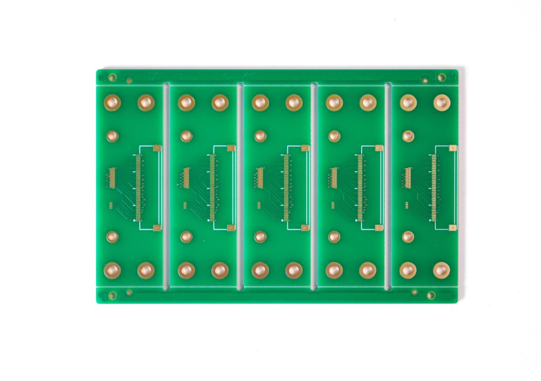
What is 16 layer PCB? Let’s discover meaning, stackup structure, thickness, technical parameter, design guide, manufacturing processes for 16 layer PCB.
Are you worried about these problems?
- How to solve high-frequency signal crosstalk in 16-layer boards?
- Can layer alignment accuracy reach В±0.05mm?
- How to achieve 7-day rapid prototyping for complex 16-layer boards?
As a multilayer PCB manufacturer, EBest Circuit (Best Technology) can provide you service and solutions:
- Step impedance design and simulation optimization: reducing signal loss by 30%, passing 10Gbps testing.
- High Precision Laser drilling: achieving В±0.03mm precision with 99.2% yield.”
- Modular panelization + flexible scheduling: enabling 7-day delivery for small batches and 40% shorter mass production cycles.
Welcome to contact us if you have any request for 16 layer PCB: sales@bestpcbs.com.
What Does 16 Layer PCB Mean?
A 16 layer PCB is a multi-layer circuit board fabricated by precisely laminating 16 conductive copper foil layers with dielectric materials. It integrates high-frequency or high-speed substrates (e.g., Rogers 4350B), laser-drilled microvias (HDI), precision impedance-controlled traces (В±5% tolerance), and electromagnetic shielding layers.
Through professional stack-up design, it achieves signal-power-ground layer isolation. Main advantages include supporting 56Gbps ultra-high-speed signaling, reducing EMI by 40%, and enabling high-density BGA component placement (10,000+ pins). Primary applications span AI accelerator cards in data centers, 5G mmWave base station modules, and advanced medical imaging systems.

16 Layer PCB Stackup
- Top/Bottom Signal Layers: Utilize low-loss materials (e.g., Rogers 4350B) with 5-10mil trace widths, strictly controlled 50О©В±10% impedance, and microstrip structures to minimize signal attenuation for high-speed transmission (e.g., 56Gbps).
- Inner High-Speed Signal Layers: Sandwiched between power and ground planes for “signal-power-ground” coupling. 3-5mil dielectric thickness reduces crosstalk and EMI, with 100О©В±10% differential pairs spaced 5-10mil apart.
- Power/Ground Planes: 1.2-2.1mil copper thickness, 5-15mil spacing with high-frequency decoupling capacitors (e.g., 100nF/1ОјF) to optimize power integrity. Ground planes act as EMI shields, reducing common-mode noise.
- Dielectric Layers: FR4 (Оµr=4.2-4.7) or high-speed substrates (e.g., Megtron6) with В±10% thickness uniformity. Glass weave avoids “window effect” for impedance consistency, bonded via prepreg.
- Blind/Buried Vias: Laser-drilled HDI vias (0.1-0.2mm diameter) connect inner layers, minimizing via stubs (≤500μm). Back-drilling optimizes signal paths, preventing impedance discontinuity.
- Thermal Management: Large copper areas, thermal vias, and heat-conductive materials (e.g., aluminum/copper substrates) dissipate heat. Power components use thermal pads to limit temperature rise ≤20℃.
- Symmetric Stack-Up: Balanced layer arrangement (e.g., signal-power-ground-signal) prevents warpage. Zig-zag or 45В° routing reduces high-frequency radiation, ensuring manufacturing yield.
How Thick Is a 16 Layer PCB?
The typical thickness of a 16-layer PCB ranges from 1.6mm to 2.4mm, depending on stackup structure, material selection, and application scenarios. For instance, the standard 1.6mm thickness suits most high-density routing needs, while 2.0-2.4mm thicknesses are often used where enhanced mechanical strength or thermal performance is required. Total thickness is determined by the combined thickness of conductive layers, dielectric layers, and prepreg, with precise lamination processes ensuring uniform layer-to-layer consistency.
16-Layer PCB Board Technical Parameter
| Technical Parameter | Parameter Value/Range |
| Layer Count | 16 layers |
| Total Thickness | 1.6mm-2.4mm |
| Copper Foil Thickness | 1.2mil-2.1mil |
| Dielectric Material Type | FR4 (Оµr=4.2-4.7), High-Speed Materials (e.g., Rogers 4350B, Megtron6) |
| Dielectric Thickness Uniformity | В±10% |
| Single-Ended Impedance Control | 50О©В±10% |
| Differential Impedance Control | 100О©В±10% |
| Trace Width Range | 5mil-10mil |
| Trace Spacing Range | 5mil-10mil |
| Blind/Buried Via Diameter | 0.1mm-0.2mm |
| Via Stub Length | ≤500μm |
| Surface Finish | ENIG, OSP, Immersion Gold, etc. |
How to Design a 16 Layer PCB?
Below is 16 Layer PCB design guide:
1. Requirements Analysis & Planning
- Define circuit functional requirements: such as high-speed signal bandwidth (56Gbps), power layer count, impedance control tolerance (В±5%).
- Determine stackup structure: recommended 4 signal layers / 6 power layers / 6 ground layers (adjustable per application).
- Plan key component placement zones: BGA footprints, connectors, and high-pin-count devices.
2. Stackup Structure Design
- Use symmetric stackup to prevent warpage: e.g., Top-S1-G1-P1-S2-S3-G2-P2-Core-P3-G3-S4-S5-P4-G4-S6-Bottom.
- Position high-speed signals adjacent to ground planes to minimize loop area.
- Place power/ground planes adjacent to form interplanar capacitance, reducing voltage ripple.
3. Material Selection
- Base material: Low-loss substrates (e.g., Isola FR408HR for controlled impedance).
- Copper foil: HVLP (Horizontal Low Profile) for signal layers to reduce skin effect losses.
- Board thickness: 2.4mm В±10% (optimized for mechanical stability and thermal dissipation).
4. Rule Setting
- Differential pair impedance: Target 100О© В±10% (verified via TDR testing).
- Minimum trace width/spacing: ≥4mil (prevents manufacturing defects).
- Blind/buried via scheme: e.g., 1-2 layer laser vias + 2-15 layer mechanical vias.
5. Layout Phase
- Prioritize placement of critical components (BGA, power modules).
- Position power modules near their respective power planes to minimize IR drop.
- Match trace lengths for high-speed signals using serpentine routing.
6. Power Integrity Design
- Apply 20H rule (power plane smaller than ground by 20x dielectric thickness) to suppress edge radiation.
- Deploy decoupling capacitors per power domain: 0.1ОјF (high-frequency) + 10ОјF (bulk) combination.
- Avoid plane splits crossing under sensitive signals to prevent noise coupling.
7. Signal Integrity Optimization
- Enforce 3W rule (minimum spacing ≥3x trace width) between aggressive/passive traces.
- Use serpentine routing for length-sensitive signals (e.g., DDR, PCIe lanes).
- Add grounding vias adjacent to signal vias to shield against crosstalk.
8. DFM (Design for Manufacturing) Checks
- Validate minimum drill size (≥8mil) for reliable plating.
- Ensure copper balance (≥30% copper coverage per layer) to prevent warpage.
- Verify solder mask bridge width (≥3mil) to avoid shorts.
9. Production File Output
- Generate Gerber 274X files with layer-specific data.
- Provide IPC-356 netlist for electrical test validation.
- Annotate special processes: back-drilling, via filling/plating.
10. Prototype Testing & Iteration
- Perform TDR impedance verification across critical traces.
- Measure power rail ripple (≤5% of nominal voltage) under load.
- Validate S-parameters using vector network analyzer (VNA) for signal integrity.
How to Make a 16 Layer PCB?
1. Panel Cutting: Raw copper-clad laminates (CCLs) are precision-cut to design dimensions ±0.2mm using automated shearing machines, with ≥5mm process margins reserved for edge handling during subsequent processing.
2. Inner Layer Imaging: Dry film photoresist is laminated, exposed via UV laser direct imaging (LDI) at 5080dpi resolution, developed, and etched to form traces with В±3Ојm line width tolerance. Post-etch AOI verifies 100% defect coverage (e.g., shorts, opens).
3. Lamination: Prepreg (PP) sheets and copper foils are stacked in symmetric sequence, vacuum-compressed at 175В±5в„ѓ under 350В±20psi pressure for 120 minutes to ensure void-free bonding and dielectric thickness uniformity В±10%.
4. Drilling: Mechanical drilling uses carbide drills (≥0.15mm diameter) with spindle speed 120kRPM and feed rate 0.5m/min. Laser blind vias (φ0.1mm) are drilled with depth control ±5μm via adaptive laser pulse modulation.
5. Hole Metallization: Chemical copper deposition (0.3-0.5μm) creates conductive seed layer; electroplating thickens hole walls to ≥25μm copper thickness, ensuring reliability per IPC-4761.
6. Outer Layer Imaging: LDI exposure defines outer layer patterns with В±15Ојm registration accuracy. Pattern plating deposits 40Ојm В±5% copper thickness, followed by solder mask application (75Ојm thickness).
7. Special Processes: Back-drilling removes via stubs to <0.15mm length using controlled-depth drilling; resin plugging fills plugged holes with <5% void ratio via vacuum impregnation.
8. Solder Mask & Surface Finish: Spray-coated solder mask (LPISM) is UV-cured; ENIG finish deposits 3-5Ојm nickel layer and 0.05-0.1Ојm immersion gold for corrosion protection and solderability.
9. Profiling: CNC routing achieves В±0.1mm dimensional tolerance; V-scoring cuts to 1/3 board thickness В±0.05mm for easy breakout, with scoring depth verified via cross-section microscopy.
10. Testing: Flying probe tests ensure 100% net connectivity; TDR verifies В±7% impedance tolerance; eye diagram analysis confirms signal integrity (e.g., 20% eye opening for 28Gbps signals).
11. Final Inspection: Thermal stress cycles (288℃ solder dip ×3 times) test for delamination; cross-section analysis verifies copper plating thickness, hole fill, and laminate integrity with ≤5% deviation.
12. Packaging: Boards are vacuum-sealed in anti-static bags with silica desiccant, housed in ESD-safe rigid containers for moisture/corrosion protection during transit.
Why Choose EBest Circuit (Best Technology) as 16 Layer PCB Manufacturer?
Reasons why choose us as 16 layer PCB manufacturer:
- 19+ Years Expertise in 16-Layer PCB Manufacturing: Proven track record of delivering high-complexity PCBs with precision engineering and innovative design solutions, backed by extensive R&D capabilities.
- Competitive Pricing Without Compromise: Top-tier quality at industry-leading prices through optimized production processes and bulk material sourcing, ensuring cost efficiency without sacrificing performance.
- No MOQ & Flexible Production Scaling: Prototypes, small batches, or mass production—all orders are accommodated with rapid turnaround times, supporting agile product development cycles.
- 99% On-Time Delivery Guarantee: Rigorous supply chain management and production scheduling ensure deadlines are met, minimizing project delays.
- ISO-Certified Quality Systems: Adherence to ISO9001 (quality), ISO13485 (medical), and IATF16949 (automotive) standards, ensuring compliance with global regulatory requirements.
- Turnkey Solution: Full-service offerings from DFM (Design for Manufacturing) consultation to PCB assembly, testing, and logistics, streamlining your supply chain.
- Advanced Technology & Material Mastery: Expertise in high-speed materials (e.g., Rogers 4350B, Megtron6), HVLP copper foil, and laser microvia technology for superior signal integrity and thermal management.
- Stringent Quality Control at Every Stage: Multi-stage inspections including AOI, X-ray drilling verification, and cross-sectional analysis to ensure zero defects and В±3Ојm line width precision.
- Sustainable Manufacturing Practices: Eco-friendly processes (RoHS-compliant materials, waste reduction) and energy-efficient equipment to minimize environmental impact.
Welcome to contact us if you have any request for 16 layer PCB design, prototyping, manufacturing, assembly: sales@bestpcbs.com.
Tags: 16 layer PCB, 16 layer PCB board