

Why choose standard copper thickness PCB? Let’s explore definition, benefits, application, thickness chart, manufacturing processes for standard copper thickness PCB.
Are you troubled with these problems?
- Why does my high-speed design always fail signal integrity tests?
- How do I reduce costs without sacrificing reliability?
- Why are my prototype lead times so long?
EBest Circuit (Best Technology) can provide service:
- First-Pass Prototyping Success – Advanced impedance control & pre-layout simulation to eliminate SI issues.
- Cost-Effective Reliability – Smart copper weight selection (1oz/2oz) balancing performance and BOM costs.
- 48-Hour Rapid Prototyping – Dedicated small-batch line for urgent verification needs.
Welcome to contact EBest Circuit (Best Technology) if you have any request for heavy copper PCB: sales@bestpcbs.com.
What Is Standard Copper Thickness PCB?
Standard Copper Thickness PCB typically refers to 1 oz (ounce) per square foot (≈35 µm) for outer layers and 0.5 oz (≈17.5 µm) for inner layers. This balance optimizes cost, manufacturability, and performance for most consumer electronics, signal traces, and low-power applications. Thicker copper (e.g., 2 oz–6 oz) is used for high-current, power, or thermal management needs. Standard thickness ensures reliability while minimizing material and processing costs.
IPC Standard PCB Copper Thickness Chart
| Copper Weight (oz/ft²) | Thickness (μm) | IPC-2152 Current Rating (1mm trace, 10°C rise) | Typical Application |
| 0.5 oz | ~17.5 μm | ~1.5A | Low-power circuits |
| 1 oz | ~35 μm | ~3A | Consumer electronics |
| 2 oz | ~70 μm | ~5A | Power supplies |
| 3 oz | ~105 μm | ~7A | Automotive, industrial |
| 4 oz | ~140 μm | ~10A+ | High-current systems |
Why Choose Standard Copper Thickness PCB?
Advantages of standard copper thickness PCB:
- Cost Optimization: Standard thickness (1 oz/ft² / 35 µm) reduces material and fabrication costs by 20–50% compared to heavy copper (≥2 oz).
- Universal Compatibility: Works with 90%+ PCB designs, including low-current signals, controlled impedance traces, and mixed-signal boards.
- Proven Reliability: Tested for decades in consumer/industrial electronics, meeting IPC-6012 Class 2 standards for electrical and thermal performance.
- Simplified Manufacturing: Avoids specialized etching or laminate requirements, ensuring faster lead times and fewer production risks.
- Design Flexibility: Enables 4–6 mil traces for high-density SMT/BGA and simplifies impedance control (e.g., 50Ω microstrip).
- Supply Chain Efficiency: Standard copper foils (ED/RA) are readily available, minimizing delays versus custom heavy copper orders.
- Thermal Performance Balance: Adequate for most applications (ΔT ≤10°C at 5A). Pair with thermal vias/copper pours for higher currents without thickening copper.
- Risk Mitigation: Avoids over-engineering risks like plating unevenness or delamination from unverified fab capabilities.
When to Use Standard Copper Thickness PCB?
- Consumer Electronics – Smartphones, tablets, and IoT devices with currents <5A. Standard copper (1 oz/ft²) balances cost and performance.
- Low-Current Signal Transmission – Sensor interfaces, microcontroller I/O, and digital communication lines (e.g., I²C, SPI) where currents <1A.
- Controlled Impedance Traces – High-speed designs (e.g., USB, HDMI, Ethernet) needing 50Ω/100Ω microstrip/stripline with predictable trace geometry.
- General Industrial Control – PLCs, relays, and low-power motor drivers (currents <10A) where thermal performance is adequate with standard copper.
- Lightweight Applications – Drones, wearables, or aerospace systems prioritizing reduced board weight over extreme current handling.
- Standard Communication Devices -Routers, modems, and Wi-Fi modules with power rails ≤12V and currents <5A.
How to Choose PCB Copper Layer Thickness?
- Current Requirements: Thicker copper (e.g., 2 oz) handles higher currents; thinner (e.g., 0.5 oz) suffices for low-power circuits.
- Signal Integrity: Thinner copper reduces skin effect for high-frequency signals; thicker copper minimizes resistance for power traces.
- Thermal Management: Thicker copper dissipates heat more effectively in high-power designs.
- Manufacturing Constraints: Standard thicknesses (0.5 oz–6 oz) are easier to fabricate; exotic thicknesses increase cost.
- Impedance Control: Thinner copper is preferred for controlled impedance traces in high-speed PCBs.
- Cost: Thicker copper raises material and production costs; optimize based on performance needs.
- Layer Stackup: Match thickness with dielectric layers to maintain consistent impedance and manufacturability.
- Via and PTH Handling: Thicker copper requires larger vias/pads to ensure reliable plating.
- Industry Standards: Follow IPC-2221 or design guidelines for typical applications (e.g., 1 oz for consumer electronics).
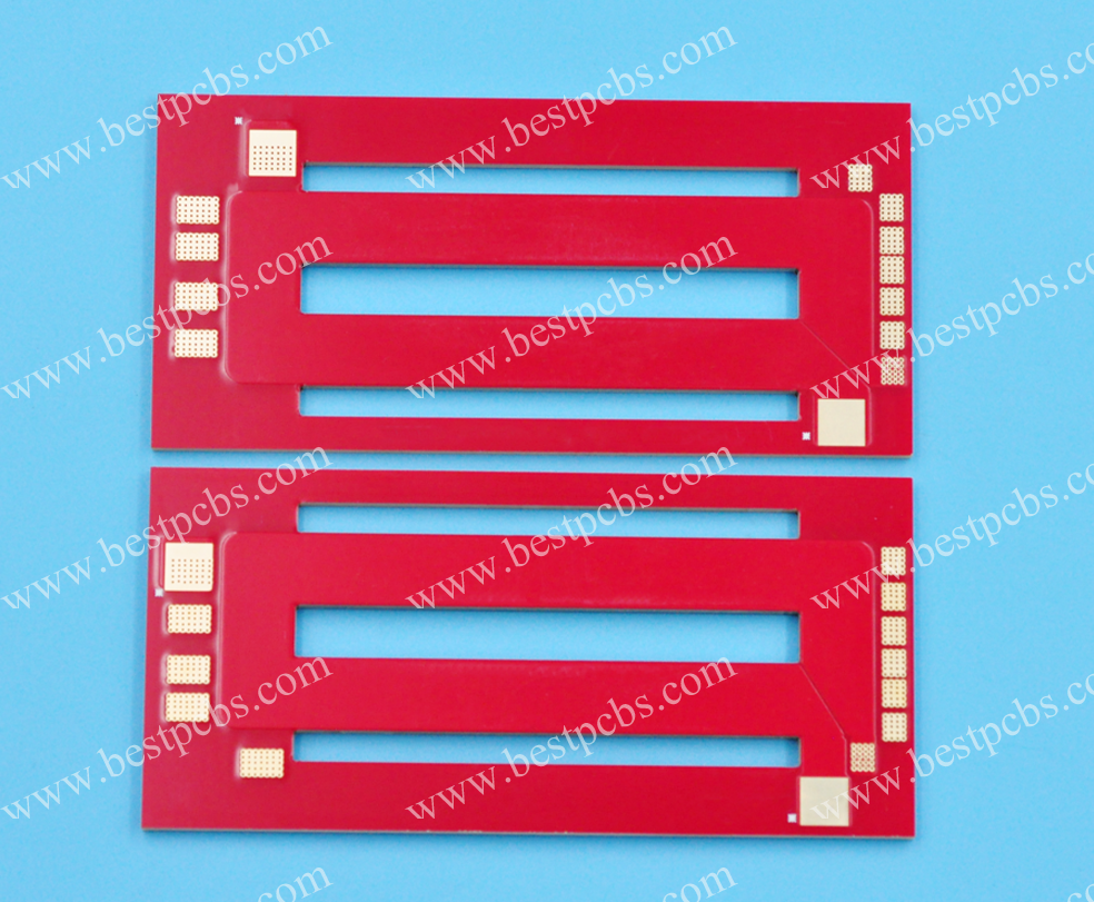
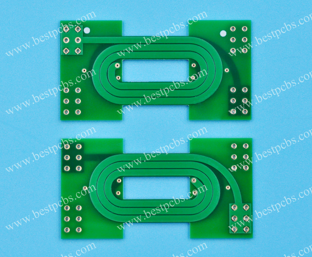
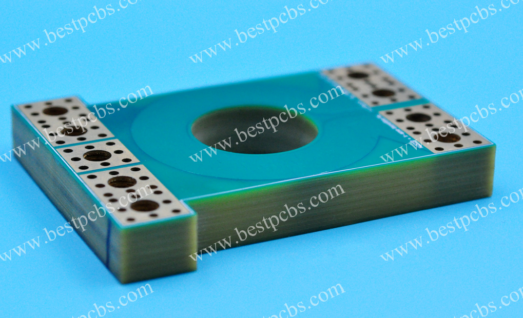
How to Make A Standard Copper Thickness PCB?
- Design PCB Layout: Use CAD software to create circuit patterns, ensuring trace widths and spacing meet standard copper thickness requirements.
- Select Copper Foil Thickness: Choose copper foil with standard thickness (e.g., 1 oz/35 µm or 2 oz/70 µm) for inner and outer layers.
- Prepare Substrate Material: Use FR-4 or similar laminate core with pre-bonded copper foil of desired thickness.
- Image Transfer (Inner Layers): Apply photoresist, expose to UV light using artwork film, and develop to transfer circuit patterns.
- Etch Inner Layers: Use chemical etching (e.g., ammonium persulfate) to remove excess copper, leaving desired traces.
- Layer Stackup: Align etched inner layers with prepreg sheets and outer copper foil, then press under heat/pressure to laminate.
- Drill Holes: Use CNC drilling to create via holes and component mounting holes.
- Electroless Copper Deposition: Apply chemical bath to deposit a thin conductive layer on hole walls.
- Electrolytic Plating: Pass current through holes to build up copper thickness (e.g., 1-2 oz) on traces and vias.
- Outer Layer Imaging: Repeat photoresist, exposure, and development steps for outer layer circuit patterns.
- Final Etching: Remove excess copper from outer layers using controlled etching to retain standard thickness.
- Solder Mask Application: Coat PCB with epoxy-based solder mask to protect copper traces.
- Surface Finish: Apply finishes like HASL, ENIG, or OSP to prevent oxidation and ensure solderability.
- Quality Inspection: Use AOI, X-ray, or microsectioning to verify copper thickness uniformity and circuit integrity.
Standard Copper Thickness PCB Manufacturer – EBest Circuit (Best Technology)
- Certified & Compliant Standards: ISO 9001, ISO 13485, IATF 16949 Certified, and UL, REACH, RoHS Compliant
- Precision Thickness Control – Strict adherence to 1oz/ft² (35μm) standard with ±5% tolerance for consistent performance.
- Competitive Pricing – Bulk-order discounts & transparent cost structure (20% lower than industry average).
- Strict Quality Inspection– 100% full inspection in mass production.
- Fast Turnaround – 24-hour expedited service available with standard 5-7 day lead time.
- Free DFM Expertise – Free design review to optimize trace widths/spacing for 1oz copper.
- Multilayer Capability – Supports up to 20-layer boards with standard copper lamination.
- Global Logistics – DHL/FedEx partnerships for door-to-door delivery in 3-5 days.
- 24/7 Support – Dedicated account managers for real-time order tracking.
Our Quality Inspection & Testing
- Visual Inspection (IPC-A-600): Mandatory for surface defects (scratches, pinholes) and solder mask alignment. Ensures compliance with Class 2/3 acceptability criteria.
- Automatic Optical Inspection (AOI): Critical for detecting trace/space violations (>4 mil) and solder mask defects. Post-etch inspection prevents short circuits.
- X-Ray Inspection (IPC-6012): Required for hidden features (blind/buried vias, BGA solder joints). Validates via integrity and void percentages (<5%).
- Electrical Continuity Test (Flying Probe/ICT): Ensures all nets are connected. Flying probe used for prototypes; ICT for high-volume production.
- Impedance Control Verification (TDR): Mandatory for high-speed designs (e.g., 50Ω traces). Tolerance must stay within ±10% (IPC-2221).
- Thermal Shock Test (IPC-TM-650): -55°C to 125°C cycling for 100 cycles. Pass criteria: no delamination or cracks.
- Humidity Resistance Test (85°C/85% RH):168-hour exposure. Insulation resistance must remain >100MΩ (IPC-TM-650).
- Solderability Test (IPC-TM-650): HASL/ENIG pads dipped in 245°C solder. Minimum 95% coverage required to ensure solder joint reliability.
- Peel Strength Test (IPC-TM-650): Copper-substrate adhesion: ≥1.4 lb/in (inner layers), ≥2.8 lb/in (outer layers). Prevents trace lifting.
- Microsection Analysis: Slicing through PTHs to verify copper thickness (±20%) and via wall plating. Ensures annular rings meet IPC-6012.
How to Get a Quote For Your PCB Project?
Required Materials Checklist:
Gerber Files
- Include all layers (copper, solder mask, silkscreen) in RS-274X format.
- Verify file accuracy with a Gerber viewer.
Bill of Materials (BOM)
- List components with part numbers, quantities, and footprints.
- Specify brand preferences for critical parts (e.g., capacitors, ICs).
Technical Specifications
- Board dimensions, layer count (e.g., 4L, 6L), and copper thickness (1 oz/2 oz).
- Surface finish (HASL, ENIG, OSP) and impedance requirements.
Fabrication Notes
- Via types (through-hole, blind/buried) and minimum trace/space (e.g., 4 mil).
- Special requirements (e.g., controlled impedance, thermal vias).
Assembly Details (If Applicable)
- SMT/PTH component placement files (Centroid/Pick-and-Place).
- Test requirements (e.g., ICT, functional testing).
Submit your requirements to us for a quote: sales@bestpcbs.com.