

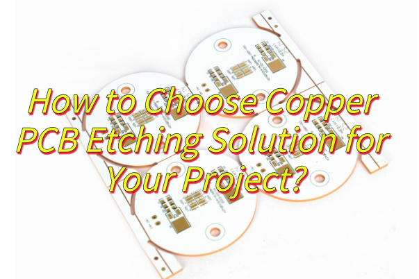
How to choose copper etching PCB solution? A guide to selecting optimal copper PCB etching solutions: methods, tolerances, and process specifications.
Are you troubled with these issues?
- When high-frequency devices are running, can your copper substrate quickly dissipate heat to avoid performance degradation?
- With traditional processes, do material waste and yield fluctuations leave you struggling to manage costs?
- When orders suddenly surge, can your supplier respond and deliver reliably within 72 hours?
EBest Circuit (Best Technology) can provide services and solutions:
- Gradient Heat Dissipation Structure: Using nano-scale copper lamination technology, thermal resistance is reduced by 40%, ensuring long-term stable operation in high-temperature environments.
- Lean Production System: Utilizing a closed-loop quality monitoring system, material utilization has increased to 92%, reducing unit costs by 15%.
- Flexible Supply Chain Network: Three factories across China collaborate, enabling 7-day delivery for regular orders and lightning-fast scheduling for expedited orders.
Welcome to contact us if you have any request for metal core PCB: sales@bestpcbs.com.
What is Copper PCB Etching?
Copper PCB etching is a critical manufacturing process that selectively removes unwanted copper from a copper-clad printed circuit board (PCB) to create precise circuit patterns. By chemically dissolving unprotected copper areas while preserving resist-coated traces, this technique transforms raw copper-clad substrates into functional electronic components. The process involves two main approaches: acidic etching (using ferric chloride or cupric chloride solutions) for cost-effective mass production, and alkaline etching (with ammonia-based solutions) for high-precision applications requiring minimal side etching. Copper-clad PCB etching must balance speed, precision, and environmental considerations to achieve optimal results in electronic fabrication.
What Solution is used to Copper PCB Etching?
Acidic Etching Solutions
- Examples: Sulfuric acid (H₂SO₄) – hydrogen peroxide (H₂O₂), acidic copper chloride (CuCl₂).
- Characteristics: Fast etching speed, low cost, and recyclable waste (copper sulfate). Suitable for inner-layer boards.
- Application: Inner-layer PCB fabrication, cost-effective small-scale production.
Alkaline Etching Solutions
- Examples: Alkaline copper chloride (Cu(NH₃)₄Cl₂), ammonia-based solutions.
- Characteristics: High etching factor (4:1), excellent for thick copper layers and fine lines. Requires oxygen injection for regeneration.
- Application: Outer-layer PCBs, high-precision HDI boards.
Ferric Chloride (FeCl₃) Solutions
- Characteristics: Low cost, stable process, but generates non-recyclable waste.
- Application: Legacy systems, low-cost hobbyist use (with proper waste disposal).
Sulfuric Acid – Nitric Acid Solutions
- Characteristics: Fast etching but produces nitrogen oxide pollutants.
- Application: Limited use due to environmental restrictions (e.g., Shenzhen’s 2025 VOC limits).
Sodium Persulfate (Na₂S₂O₈) Solutions
- Characteristics: High oxidizing power, precision cleaning for metal surfaces.
- Application: Advanced metal processing (e.g., semiconductor, aerospace).
Sulfuric Acid – Hydrogen Peroxide Solutions
- Characteristics: Eco-friendly, recyclable, and cost-effective.
- Application: General-purpose PCBs, compliance with 2025 environmental regulations.
How to Choose Copper PCB Etching Solution?
Strategies for Selecting Copper PCB Etching Solution:
Production Scale Alignment
- Large-Scale Production: Prioritize for alkaline copper chloride etchants. They offer the fastest etching speed (2.0–2.5 mil/min) and a high etch factor (4:1), ideal for high-throughput scenarios and thick copper layers.
- Small-Scale/Hobbyist Use: Choose sulfuric acid–hydrogen peroxide solutions. They are cost-effective (1/3 the cost of ferric chloride), eco-friendly (produce only copper sulfate waste), and support copper recovery for sustainability.
MCPCB Type Compatibility
- Inner Layer Boards: Use acidic copper chloride etchants. Their simple chemistry and wide parameter window ensure stable performance with minimal maintenance, suitable for stable inner-layer processes.
- Outer Layer Boards: Select alkaline copper chloride etchants. They avoid reacting with tin/tin-lead solder masks, preserving line integrity during etching.
Environmental Compliance
- Prioritize sulfuric acid–hydrogen peroxide solutions. They generate non-toxic byproducts (copper sulfate) and align with strict 2025 regulations. Avoid ferric chloride due to pollution and disposal challenges.
Cost Efficiency
- Low-Cost Needs: Sulfuric acid–hydrogen peroxide and ferric chloride are budget-friendly. Ferric chloride, however, incurs long-term costs due to regeneration difficulties.
- High-Performance Demands: Sodium persulfate etchants excel in precision cleaning (e.g., metal surface contaminants) but are costly. Use for niche applications requiring oxidative power.
Operational Simplicity
- Easy Maintenance: Acidic copper chloride requires minimal intervention, with a broad parameter tolerance. Ideal for users prioritizing simplicity.
- Complex Processes: Alkaline copper chloride demands oxygen injection and tight parameter control. Suitable for experienced operators in specialized settings.
Safety Considerations
- All etchants are corrosive; use PPE (gloves, goggles). Sulfuric acid–hydrogen peroxide requires secure storage of hydrogen peroxide (oxidizing agent).
Quality Requirements
- Fine-Line Precision: Alkaline copper chloride delivers superior sidewall verticality and etch factor, critical for HDI/high-density boards.
- General-Purpose: Sulfuric acid–hydrogen peroxide or ferric chloride suffice for standard designs.
What Are Types of Copper Clad PCB Etching?
Spray Etching
- Etchant is propelled via nozzles onto the PCB, ensuring rapid and even copper removal. Adjustable pressure and nozzle design allow customization for fine-pitch circuits. Common in industrial setups for consistent line widths.
Dip Etching (Immersion Etching)
- PCBs are fully submerged in an etchant bath. Mechanical stirring or pumped circulation prevents solution stratification. Cost-effective for low-volume production but requires precise time-temperature control to avoid over-etching.
Air Bubble Etching
- Air is injected into the immersion tank, creating bubbles that agitate the etchant. This reduces “etch-factor” variability and improves edge definition in complex geometries. Effective for multi-layer boards with tight tolerances.
Electrochemical Etching
- Anodic dissolution accelerates copper removal using direct current. The PCB serves as the anode in a conductive solution (e.g., copper sulfate). Enables precise depth control and reduces chemical waste. Ideal for selective etching tasks.
Laser Direct Etching (LDE)
- Focused laser beams vaporize copper without resist layers. Supports ultra-fine traces (<50µm) and flexible design changes. Minimal chemical use but demands high capital investment. Used in advanced HDI and flexible PCBs.
Horizontal Conveyorized Etching
- Automated systems transport PCBs horizontally through staggered spray zones. Combines speed with precision, optimizing etchant renewal. Suited for high-throughput manufacturing of double-sided and multilayer boards.
What is the Etching Tolerance of Copper PCB?
The etching tolerance of copper PCBs depends on the etching method and copper thickness: wet etching (chemical) typically achieves ±3–5μm for standard 1–2oz copper, while dry etching (plasma/laser) can reach ±0.5μm for ultra-fine lines in HDI/5G applications. Thicker copper (≥3oz) increases side-etching, requiring pulse etching to maintain ±8% linewidth tolerance. Main factors include etchant type (alkaline > acidic precision), temperature control, and process optimization.
Copper PCB Etching Specification
| Parameter | Specification | Notes |
| Etching Method | Wet (Chemical) / Dry (Plasma/Laser) | Wet: ±3–5μm tolerance; Dry: ±0.5μm for HDI/5G PCBs. |
| Copper Thickness | 1oz (35μm) – 3oz (105μm) | Thicker copper increases side-etching; optimize pulse etching for ≥3oz. |
| Etchant Type | Ferric Chloride (FeCl₃) / Ammoniacal Copper ([Cu(NH₃)₄]²⁺) | Alkaline etchants offer finer control (±0.5μm) but require temperature stability. |
| Temperature Range | 45–55°C (Alkaline) / 30–50°C (Acidic) | ±1°C precision critical for consistency. |
| Etching Time | 2–8 minutes (varies by copper thickness) | Automated spray systems reduce time by 30% vs. immersion. |
| Side-Etch Factor | ≤8% of linewidth (3σ control) | Laser/plasma etching achieves <5% for micro-traces. |
| Residual Copper | ≤0.5μm (post-etch inspection via SEM) | Critical for high-frequency signal integrity. |
| Waste Management | Neutralization tanks for FeCl₃; ammonia scrubbers for alkaline etchants | Compliance with IPC-1401 standards. |
What is the Process of Copper PCB Etching?
1. Design Preparation
- Convert PCB layout files (e.g., Gerber) into photomasks using specialized software.
- Ensure design accuracy for trace widths, spacing, and layer alignment.
2. Substrate Cleaning
- Clean copper-clad laminate (CCL) to remove contaminants (oils, oxides) using alkaline solutions.
- Roughen copper surfaces via mechanical brushing or chemical treatments to enhance adhesion.
3. Photoresist Application
- Coat the CCL with a liquid or dry film photoresist, which acts as a protective layer during etching.
- Dry film photoresist is laminated under heat/pressure for uniform coverage.
4. Exposure & Development
- Align photomasks with the CCL and expose to UV light, hardening the resist in exposed areas.
- Develop unexposed resist using alkaline solutions (e.g., K2CO3), leaving only the desired copper traces protected.
5. Etching Process
- Spray Etching: Spray ammonia-based etchant (e.g., CuCl2) onto the board to dissolve exposed copper.
- Dip Etching: Submerge the board in an agitated etchant bath for uniform copper removal.
- Control parameters: temperature (45–55°C), spray pressure, and etchant concentration.
6. Resist Stripping
- Remove remaining photoresist using NaOH or proprietary stripping solutions.
- Ensure no resist residues remain to prevent adhesion issues in subsequent steps.
7. Inspection & Quality Control
- Use Automatic Optical Inspection (AOI) to detect defects (e.g., under-etching, shorts).
- Perform electrical testing (e.g., flying probe) to verify connectivity.
8. Surface Finishing
- Apply protective coatings (e.g., HASL, ENIG) to prevent oxidation and enhance solderability.
- Cut PCBs to specified dimensions using CNC routing or laser cutting.
Why Choose EBest Circuit (Best Technology) as Copper PCB Manufacturer?
- 24 Hours Rapid Prototyping: Accelerates time-to-market by delivering functional prototypes within a day, enabling immediate testing and design refinement.
- Two Weeks Mass Production Turnaround: Reduces production lead time by 70%+, ensuring timely fulfillment of large orders without compromising quality.
- Thermal Performance Optimization: Prevents overheating-related failures in end products, enhancing reliability for high-power applications.
- Strict Quality Inspection: Minimizes post-delivery defects with AQL 0.65 standards, reducing warranty costs and customer complaints.
- Competitive Price: Lowers procurement expenses by 15–20% through optimized material usage and vertical integration.
- Free DFM: Avoids costly production delays by identifying design flaws early and streamlining manufacturability.
- ISO/RoHS/REACH/UL Compliance: Simplifies global market access with pre-certified products, avoiding legal risks.
- 19 Years of Experience: Ensures reliable execution of complex PCB designs (e.g., HDI, flexible circuits) with proven technical expertise.
Welcome to contact us if you have any request for copper base PCB: sales@bestpcbs.com.
Tags: copper clad pcb etching, copper pcb etching, copper pcb etching solution