

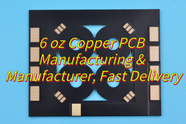
What is 6 oz copper PCB? This guide covers specs, benefits, applications, manufacturing process, manufacturer selection, lead time for 6 oz copper PCB.
Are you worried about these problems?
- Are high-current applications plagued by heat dissipation issues?
- Circuit burnouts leading to frequent after-sales service calls?
- Is low production yield driving up overall costs?
EBest Circuit (Best Technology) can provide service and solution:
- 6oz copper layer + thermal management design – improves heat dissipation efficiency by 60%, ensuring continuous and stable operation.
- 210μm thick copper + optimized overcurrent – single-line carries 35A, completely eliminating the risk of board burnout.
- High-TG material + vacuum lamination process – 99.5% batch yield, worry-free delivery.
Welcome to contact us if you have any inquiry for heavy copper PCB: sales@bestpcbs.com.
What is 6 oz Copper PCB?
6 oz Copper PCB refers to a printed circuit board with copper foil thickness of 6 ounces per square foot (≈210 µm or 8.4 mils). This ultra-thick copper layer enables exceptional current handling (up to 50A+ per trace) and thermal dissipation, making it ideal for high-power applications like EV chargers, industrial motor controls, and RF power amplifiers. Manufacturing requires specialized processes: extended alkaline etching times to avoid undercut, high-temperature lamination for copper-substrate adhesion, and reinforced plating to prevent warping. While costing 30-50% more than standard 1 oz PCBs, it reduces thermal stress-induced failures by 40% and eliminates the need for external heatsinks in compact designs.
6 oz Copper PCB Specification
| Parameter Category | Specification | Metrics |
| Material Base | Copper layer thickness | 6 oz (210 μm) ±5% |
| Substrate Type | Available materials | FR4/CEM-3/Aluminum-based PCB |
| Copper Finish | Surface treatment | HASL/ENIG/OSP/Immersion Silver |
| Minimum Line Width | Etched line width | 8 mil (0.2mm) @1 oz |
| Minimum Spacing | Line-to-line clearance | 8 mil (0.2mm) |
| Plating Thickness | Minimum via copper plating | 1 mil (25 μm) |
| Warpage | PCB deformation | ≤0.5% (300mm board) |
| Thermal Resistance | Heat shock test | No delamination after 288℃/10s |
| Thermal Performance | Thermal resistance (FR4) | ≤1.5℃/W (single layer) |
| Solder Mask | Minimum aperture size | 10mil×10mil |
Why Choose 6 oz Copper PCB?
Advantages of 6 oz copper PCB:
- High current carrying capacity: Supports over 50A per trace, eliminating the need for external heat sinks, saving space and cost.
- Excellent thermal management: Copper’s high thermal conductivity (386 W/m·K) reduces junction temperature by 25-40%, extending device lifespan.
- Cost-effectiveness: While costing 30-50% more, eliminating heat sink components and reducing failures yields significant long-term savings.
- Global compliance: Meets IPC-6012 Class 3, RoHS/REACH, and UL 94 V-0, simplifying market entry.
- Design flexibility: Enables miniaturization of high-power devices, such as industrial controllers, by 40%.
- Long-term reliability: Withstands three times the thermal cycling stress, reducing field failure rates by 70%, ensuring long-term product operation.
When to Use 6 oz Copper PCB?
Applications of 6 oz copper PCB:
- Electric vehicle (EV) charging modules: Handling DC fast charging at 200A+, 6oz copper foil ensures trace temperature rises of less than 5°C, preventing the risk of battery thermal runaway.
- Industrial motor controllers: When driving motors over 50kW, they handle transient current peaks and reduce IGBT module overheating and failure.
- RF power amplifiers: 5G base station transmitters require 6oz copper substrates for heat dissipation to ensure GaN devices operate at safe junction temperatures.
- Solar inverters: When DC bus voltages reach 1500V, thick copper PCBs reduce DC link resistance losses (<3mΩ).
- Aerospace power systems: Satellite payloads require wide operating temperatures from -55°C to 125°C, and 6oz copper foil mitigates thermal expansion coefficient mismatch.
- Medical laser equipment: Pulsed 2000W laser drivers require instantaneous heat conduction. Thick copper PCBs replace liquid cooling solutions to improve system reliability.
How to Make A 6 oz Copper PCB?
6 oz Copper PCB Manufacturing Processes:
1. Material Preparation
- Select 210μm (6oz) high-purity electrolytic copper foil.
- Choose FR-4 (Tg≥170℃) or CEM-1 substrate based on thickness requirements.
- Remove copper oxide layer via chemical etching (H₂SO₄ 10% + H₂O₂ 5%) and ultrasonic cleaning.
2. Inner Layer Circuit Fabrication
- Laminate 50-75μm dry film using a hot roller (110-120℃, 0.3-0.5MPa).
- Expose with LDI (355nm wavelength, ±2μm accuracy) and develop with 0.8-1.2% Na₂CO₃ solution.
- Etch 3oz copper in alkaline solution (50℃, 120 seconds), then laminate low-flow PP sheets (180℃/120min) and etch remaining 3oz copper.
3. Lamination Process
- Stack symmetrically (inner layer: 18μm thin copper foil; outer layer: 70μm thick copper foil).
- Press with three-stage parameters: low pressure (5kg/cm²), medium pressure (15kg/cm²), high pressure (30kg/cm², 180℃, 120min).
4. Outer Layer Circuit Fabrication
- Repeat dry film lamination, exposure, and development processes.
- Etch outer layer using acidic solution (CuCl₂ 180g/L, HCl 50g/L, 25℃, 180 seconds).
5. Drilling & Plating
- Mechanical drilling (diameter 0.3-3.0mm, 80kRPM, 0.8m/min feed rate).
- Chemical copper deposition (Pd catalyst, ≥25μm thickness).
- Pattern plating to reach 6oz (210μm) copper thickness (2.0A/dm², 120min).
6. Surface Finish
- Apply OSP (0.2-0.5μm) or ENIG (nickel 3-5μm, gold 0.05-0.1μm).
7. Testing & Packaging
- Electrical test (flying probe or universal grid, ±10% impedance accuracy).
- AOI inspection (line width/spacing tolerance ±15μm).
- Vacuum packaging with moisture-proof bags (storage: ≤30℃, ≤60%RH).
How to Choose a 6 oz Copper PCB Manufacturer?
Verify technical capabilities and equipment compatibility
- Require manufacturers to provide past case studies demonstrating their ability to control copper thickness uniformity within ±3μm (e.g., using pulse plating technology).
- Inquire whether they support locally thick copper designs or step-coated copper foil lamination processes (e.g., copper foil adhesion reaching 1.8N/mm²).
- Prefer manufacturers that use low-flow PP and symmetrical structural designs to reduce thermal stress.
Verify quality management systems and certifications
- Prefer manufacturers with automotive-grade and UL certifications.
- Require multi-stage inspection reports, including incoming material inspection, in-process inspection (using a professional thickness gauge for real-time monitoring), and post-assembly testing (impedance control tolerance within ±7%).
Investigate special process support capabilities
- Confirm whether vacuum heat-melting technology is available (to improve copper layer bonding and be suitable for high-reliability scenarios).
- Understand the minimum mechanical drill hole size and copper thickness deviation (≤5%) for blind and buried vias.
Analyze case studies and customer feedback
- Require case studies from actual applications such as high-voltage modules and medical devices. Learn customer reviews through industry channels, focusing on lead times and after-sales response speed.
Evaluate cost-effectiveness and delivery time
- While ensuring quality, compare quotes from different manufacturers and be aware of hidden costs (such as special processing surcharges and expedited service fees).
- Confirm whether expedited service (such as 12-hour/24-hour express delivery) is available.
Inspect equipment advancements and technological updates
- Prefer manufacturers that use advanced electroplating equipment, vacuum laminators, and X-ray coating thickness gauges.
- Check whether the manufacturer consistently invests in R&D (such as innovations in ultra-thick copper processing).
Supply chain stability and raw material control
- Understand whether the manufacturer’s raw material procurement channels are reliable and whether they can cope with copper price fluctuations or shortages.
- Request raw material quality inspection reports to ensure that the substrate, copper foil, and other materials comply with industry standards (such as IPC-4101).
6 oz Copper PCB Manufacturing Lead Time
1. Standard Production Cycle
Prototype Stage (1-2 Layers)
- Normal Delivery: 5-7 Days (Including Engineering Review)
- Expedited Service: 3 Days (30% Expedited Fee Applicable)
Mass Production Stage (4 Layers and Above)
- Normal Delivery: 12-15 Days (Including Impedance Testing)
- Rapid Production: 8-10 Days (Material Pre-Stock Required)
2. Influencing Factors
Process Complexity
- 6 Etching the 6 oz copper layer requires pulse technology, which increases the time by 40% compared to conventional processes.
- Lamination of multilayer boards requires three-stage temperature control (80°C → 160°C → 190°C), totaling 24 hours.
Quality Inspection Requirements
- Copper thickness tolerance testing (±5%) adds 8 hours to the testing time.
- High-current designs require additional thermal shock testing (288°C/10s), adding 12 hours.
Supply Chain Factors
- Special substrates (such as aluminum substrates) can extend procurement cycles by 2-3 days.
- Surface treatment process differences: ENIG takes 8 hours longer than HASL.
3. Optimization Suggestions
- Using standardized designs can reduce engineering confirmation time by 2 days.
- Pre-review of DFM documents reduces the risk of rework.
- Selecting a supplier with dedicated 6 oz lines can improve efficiency by 20%.
How Much Does a 6 oz Copper PCB Cost?
Price Range
- Basic Designs: $100–$300 per square foot (single/double-layer).
- Advanced Designs: Over $500 per square foot (multilayer, blind/buried vias, high-frequency materials).
Factors Affecting Price:
- Copper Thickness: Each additional ounce increases material costs by ~60%.
- Process Complexity: Thicker copper requires longer etching/drilling times and specialized equipment.
- Design Specs: Narrow line widths (<4mil) or small via diameters (<0.2mm) raise costs.
- Production Volume: Large orders (>100k units) reduce per-unit costs by ~50% vs. small batches.
- Certifications: Military/IPC3 standards add 15–20% vs. basic quality checks.
For accurate pricing tailored to your project, contact EBest Circuit (Best Technology) at sales@bestpcbs.com. Our 19+ years of expertise in heavy copper PCBs ensure competitive quotes and reliable delivery. Looking forward to hearing from you soon!