

What is a 4-layer rigid flex PCB? Let’s explore its stackup, thickness, benefits, applications, design guide and manufacturing processes through this blog.
Are you troubled with these issues?
- Is the line impedance fluctuation exceeding the standard after the product is bent? (Precision impedance control is used on rigid-flex boards, ensuring fluctuations of <5% after bending)
- Is stress concentration causing cracking during multi-module assembly? (A four-layer stepped transition design distributes 90% of mechanical stress)
- Is crosstalk severe during high-speed signal transmission? (Embedded shielding layer + differential pair routing, crosstalk suppression -50dB)
EBest Circuit (Best Technology) can provide service:
- Intelligent DFM Platform: Automatically detects design flaws and generates 3D assembly simulation videos
- Hot-Compression Process Library: Provides six compression profiles, increasing yield to 99.2%
- Full-Process Dashboard: Real-time display of 12 process statuses, including substrate cutting, lamination, and electroplating
Welcome to contact us if you have any request for rigid flex PCB: sales@bestpcbs.com.
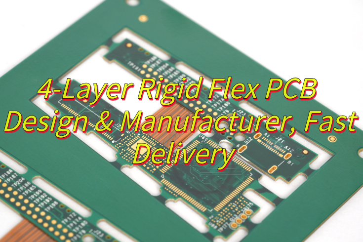
What Is a 4-Layer Rigid Flex PCB?
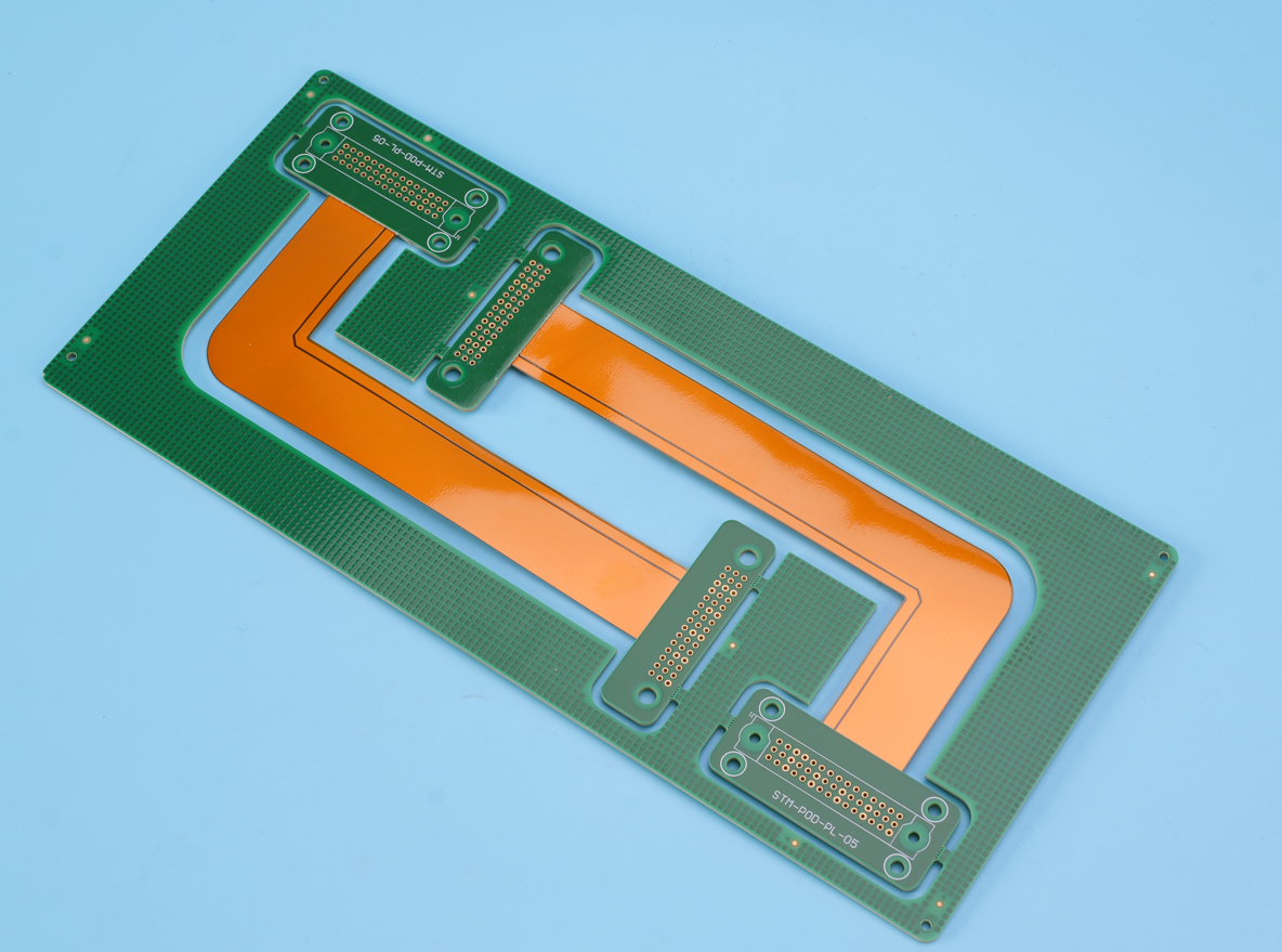
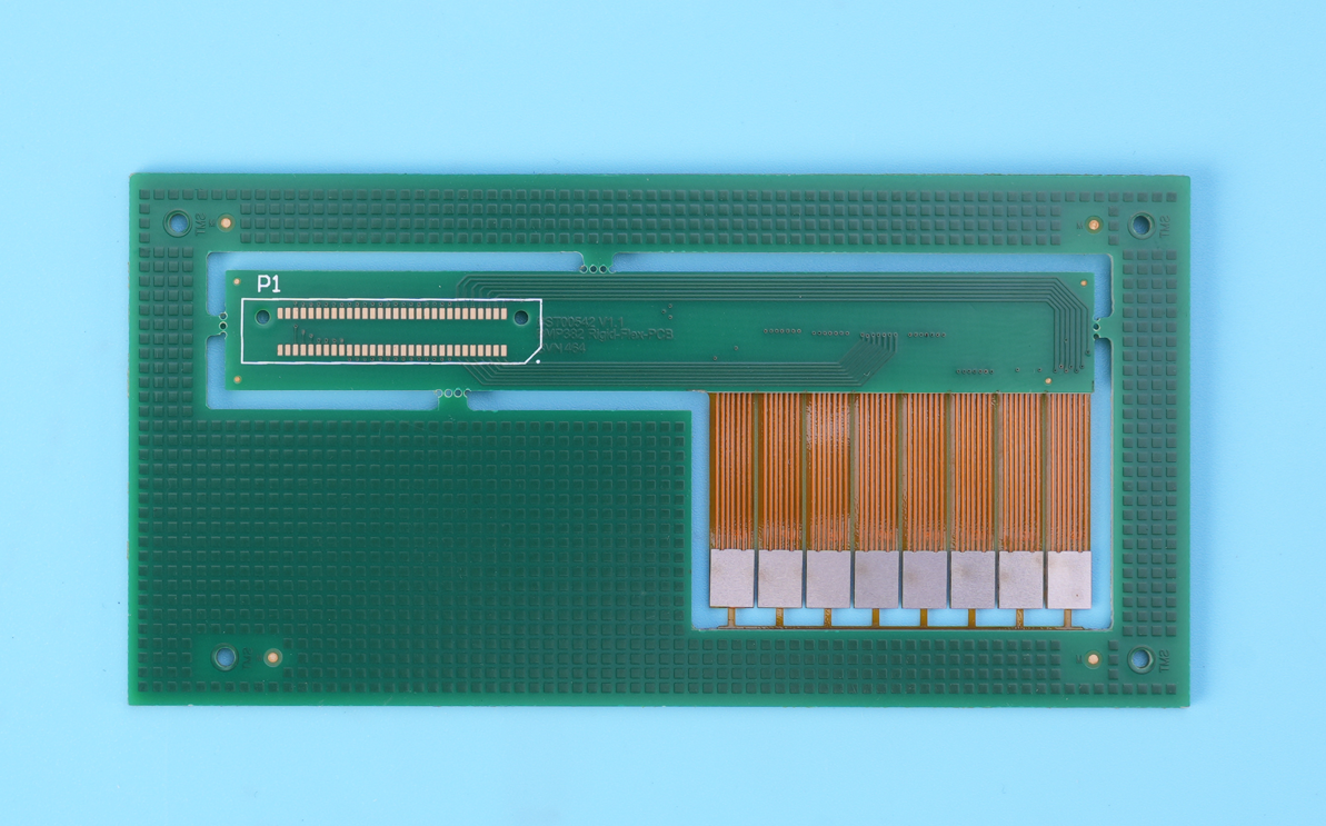
The 4-Layer rigid flex PCB is a composite board made by combining a flexible printed circuit board (FPC) and a rigid printed circuit board (PCB) through a special process, which has the characteristics of both. Its core structure usually includes a four-layer design, with the middle two layers being flexible areas and the two sides being rigid areas. The rigid-flex combination is achieved through a lamination process.
4 Layer Rigid Flex PCB Stackup
- Layer 1 (Top): Rigid signal layer (routing + key components)
- Layer 2 (Inner Layer 1): Flexible ground layer (PI substrate, providing shielding and mechanical support)
- Layer 3 (Inner Layer 2): Flexible signal layer (low-speed/auxiliary signals, optimizing routing density)
- Layer 4 (Bottom): Rigid power/ground plane (FR4, reducing noise coupling)
How thick is a 4-Layer Rigid Flex PCB?
A 4-layer rigid-flex PCB typically has a total thickness range of 0.8mm to 1.6mm, depending on the design requirements and material combinations. Rigid sections (FR4) usually measure 1.2mm thick, providing structural support. Flex sections (polyimide) are much thinner, commonly 0.1mm, allowing bending and flexibility. The overall thickness is influenced by the copper weight (e.g., 1oz for signal layers, 2oz for power/ground planes) and dielectric material (FR4 or prepreg) used in the stackup.
Why Use 4-Layer Rigid Flex PCB?
Advantages of 4-layer rigid flex PCB:
- Space and Routing Optimization: A layered design separates signal and power planes, increasing wiring density and making it suitable for compact devices like smartphones.
- Signal and Electromagnetic Performance: Adjacent power/ground layers reduce noise, and thick inner copper ensures stable high-speed signal transmission.
- Efficient Thermal Management: The inner copper foil evenly dissipates heat, and thermal vias enhance reliability in high-temperature environments.
- Mechanical and Durability: A rigid-flexible structure reduces bending failures, and a multi-layered, vibration-resistant design is suitable for industrial applications.
- Design and Cost Balance: Customized stacking optimizes performance and cost, while eliminating cables and streamlining the assembly process.
When to Use 4 Layer Rigid Flex PCB?
Applications of 4 Layer Rigid Flex PCB:
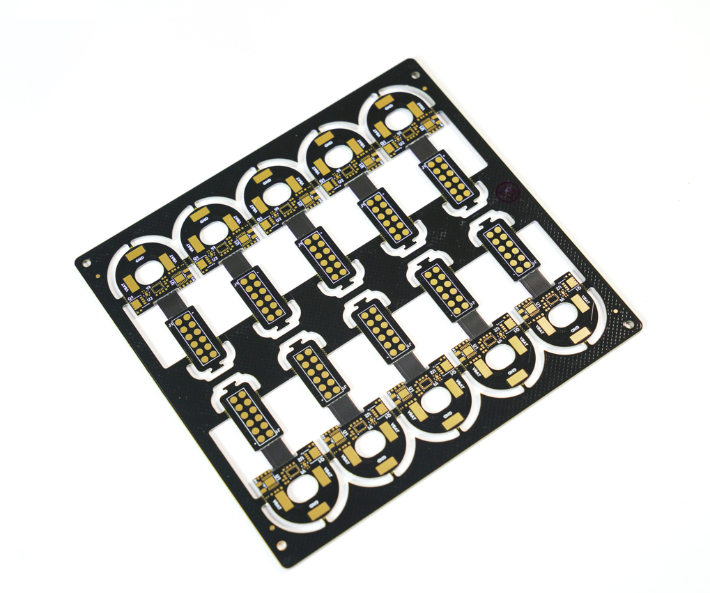
- High-Density Electronic Devices – Smartphones, tablets, and wearables requiring compact layouts with dynamic bending zones.
- Automotive Electronics – Dashboard control units and sensors exposed to vibration and temperature fluctuations.
- Medical Devices – Implantable monitors and portable diagnostics needing lightweight, biocompatible designs.
- Aerospace Systems – Avionics and satellite components demanding weight reduction and shock resistance.
- Industrial Robotics – Articulated arms with repeated motion joints requiring durable yet flexible interconnections.
- Consumer Electronics – Foldable displays and rotating-camera mechanisms necessitating 3D PCB solutions.
How to Design a 4-Layer Rigid Flex PCB?
Here are 4-layer rigid flex PCB design guide:
1. Layer Stackup & Material Selection
- Rigid Zones: Use FR4 substrate (1.6mm thickness) for structural integrity.
- Flex Zones: Opt for polyimide substrates (e.g., DuPont Pyralux AP/LF/FR) with 0.1–0.3mm thickness to accommodate dynamic bending.
- Copper Type: Rolled Annealed (RA) copper for flex layers to ensure ≥100,000 bend cycles.
- Coverlay: Match coverlay thickness to copper weight (0.5oz Cu → 1mil coverlay; 1oz Cu → 1.5mil coverlay).
2. Bend Radius Calculation
- Formula: Minimum bend radius R=t×K, where t = total flex-zone thickness, K = layer-dependent coefficient (single-layer K=6–10; dual-layer K=10–15; four-layer K=20–50).
- Example: For a 0.29mm four-layer flex zone, dynamic bend radius must be ≥5.8mm to prevent copper cracking.
3. Routing & Impedance Control
- Signal Layer Allocation: Place high-speed signals (e.g., DDR, PCIe) on outer layers (L1/L4); use inner layers (L2/L3) for power/ground planes.
- Trace Rules: Follow IPC-2223 standards (e.g., 70µm trace width/90µm spacing for 0.5mm BGA).
- Microvias: Use laser-drilled microvias (≤0.1mm diameter) with copper-filled construction (IPC-4761 Type VII).
4. Mechanical & Thermal Design
- Transition Zones: Implement “key-and-slot” designs or plastic frames to reduce stress concentration at rigid-flex junctions.
- Thermal Management: Use ≥1oz copper in power/ground planes; add thermal via arrays (spacing ≤1mm) for heat dissipation.
- Component Reinforcement: Add stiffeners (Kapton or aluminum, <10mil thickness) under flex-zone components to mitigate soldering stress.
5. Manufacturing & Testing Standards
- IPC Compliance: Meet IPC-6013 Class 3/A requirements via 100% electrical testing, AOI, and X-ray inspection.
- Reliability Tests: Conduct thermal shock (-40°C to 125°C), vibration (≥20G random), and bend cycle (≥1000 iterations) validations.
How to Make a 4-Layer Rigid Flex PCB?
Below are 4-Layer rigid flex PCB manufacturing processes:
Flexible Circuit (Flex) Processing
1. Shearing: Cut raw flex material (e.g., polyimide w/ copper) to size.
2. Drill: Use CNC to drill holes for layers/connections (4 – layer flex → holes for interlayer links).
3. PTH: Plate copper inside drilled holes (electro/electroless plating) for layer connectivity.
4. Dry Film Lamination: Apply photosensitive dry film (heat/pressure) as etching mask.
5. Develop: UV – expose film, wash off unexposed areas.
6. Etch: Remove unmasked copper (acid bath) to form traces.
7. Strip: Chemically remove remaining dry film.
8. AOI: Scan for defects (opens, shorts, wrong trace widths) via automated optical inspection.
Rigid Circuit (Rigid) Processing
1. Shearing: Trim raw rigid material (e.g., FR – 4) to panel size.
2. Drill: CNC – drill holes for components/vias.
3. Dry Film Lamination: Apply dry film (heat/pressure) as etching mask.
4. Develop: UV – expose, wash unexposed film.
5. Etch: Acid – etch unmasked copper to create traces.
6. Strip: Remove leftover dry film.
7. AOI: Check for defects (bad traces, opens/shorts) with automated optics.
Flex + Rigid Integration
1. 2nd Drill: Add holes for final connections (flex – rigid alignment, new vias).
2. De – Burr: Remove drill burrs (brush/chemical).
3. De – smear: Clean drill residues from holes (solvent/plasma).
4. PTH: Plate copper in new holes (electro/electroless) for cross – layer links.
5. DES: Repeat develop/etch/strip to shape integrated traces (flex + rigid).
6. AOI: Verify no misalignments/shorts between flex + rigid sections.
7. Solder mask: Apply liquid polymer, UV – expose, develop to protect non – solder areas.
8. Surface Finish: ENIG/ HASL
9. Silkscreen: Print ink (stencils) for labels, part markers.
Final Assembly
1. 2nd Pressing: Bond stiffeners (if needed) via heat/pressure.
2. Flex + Rigid Align: Use fixtures/optics to align flex + rigid sections.
3. FQC: Final visual/dimensional check (no misalignments, good solder mask).
4. Coverlay: Laminate protective film (polyimide) on flex areas (heat/pressure).
5. 2nd Drill: Add final holes (connectors, mounting).
6. Outline Rout: Cut board to final shape (CNC routing/punching).
7. PCB Separate: Split multi – panel boards (routing/punching).
8. E – Test: Check for opens/shorts/impedance issues.
9. Stiffener Attach: Add mechanical supports (if needed) to flex zones.
10. Packing: Seal in anti – static bags/trays (protect from damage/ESD).
Why Choose EBest Circuit (Best Technology) as Rigid Flex PCB Manufacturer?
- International Certifications: ISO 9001/UL/IATF 16949/RoHS certified, with medical-grade ISO 13485 support.
- High-End Technical Capabilities: Supports 32-layer board design with a minimum line/space width of 0.0762mm, compatible with HDI and high-frequency materials (such as Rogers RO4350B).
- High-Quality Materials: The flexible area utilizes DuPont polyimide substrate with rolled copper (≥100,000 flex cycles) to ensure durability.
- Strict Quality Inspection: 100% electrical testing + AOI + X-ray inspection, compliant with IPC-6013 Class 3/A, with impedance control accuracy of ±5%.
- 24 Hours Rapid Prototyping: Standard orders are completed within 7 days, expedited orders within 3 days, with two free prototype verifications per month.
- Flexible Custom Design: Supports 4-layer rigid + 2-layer flex stack-ups, blind and buried vias, metal edges, and other special processes.
- Free Technical Support: Design-for-Function (DFM) checks and optimization, with 24/7 engineer assistance for impedance matching and thermal management.
- Cost-effective solution: Tiered pricing for bulk orders (e.g., 6-ply panels at $200/10), and intelligent panelization reduces material waste by 15-20%.
- End-to-End Service: Support rigid-flex PCB prototyping, design, manufacturing, assembly service and help you reduce time and production cost a lot.
Our Rigid-Flex PCB Capabilities
| Parameter Category | Parameter Name | Parameter Value |
| Flexible Layer Count | Layer Range | 1-10 layers |
| Configuration | Bonded or Air Gap | |
| Rigid Layer Count | Layer Range | 1-40 layers |
| Total Layer Count | Layer Range | 2-50 layers |
| Flexible Core Material | Material Type | Polyimide (PI) |
| Thickness Range | 0.5 mil to 4 mils | |
| Adhesive Construction | Adhesive or Adhesiveless | |
| Copper Thickness | Flexible Circuit | 1/3 oz – 2 oz (RA or ED Copper Foil) |
| Rigid Circuit | 0.5 oz to 10 oz | |
| Coverlay | Material Type | Polyimide (PI) |
| Thickness Range | 0.5 mil to 2 mils | |
| Stiffener Material | Material Type | Polyimide (PI), FR4, Stainless Steel, Aluminum |
| Rigid Material | Material Type | FR4 (TG 130/170/180), Low Flow Prepreg |
| EMI/RF Shielding | Shielding Film | EMI/RF Shielding Films |
| Special Via Structures | Blind Vias & Buried Vias | Supported |
| Any Layer Interconnect | Supported | |
| Controlled Impedance | Impedance Values | 50Ω, 90Ω, 100Ω, 110Ω, and Custom Values |
| Surface Finishing | Process Types | ENIG, ENEPIG, Gold Plating, Gold Fingers (3-30µ” Au), Immersion Silver |
| IPC Standard | Certification Levels | IPC 6013 Class II & Class III Available |
How Can I Get a Quote for a 4 Layer Rigid-Flex PCB?
Essential Documents to Submit for Quotation
1. Gerber Files
- Include all layers (L1-L4) in 274X format with drill files.
- Specify rigid/flex zones and bend areas in layer notes.
2. Stackup Diagram
- Detail material thickness (e.g., FR4 for rigid, polyimide for flex).
- Copper weight (e.g., 1oz inner layers, 0.5oz flex zones).
3. Technical Specifications
- Board dimensions (±0.1mm tolerance).
- Min. trace/space (e.g., 4/4mil for rigid, 5/5mil for flex).
- Surface finish (e.g., ENIG, immersion gold).
4. Special Requirements
- Impedance control (e.g., ±10% for 50Ω signals).
- Stiffener locations (e.g., FR4 at connector areas).
5. Quantity & Lead Time
- Prototype (5-10pcs) or bulk order (e.g., 1k pcs/month).
- Urgency (standard 15 days or expedited 7 days).
Contact EBest Circuit (Best Technology) with your project details for a competitive quote for rigid-flex PCB needs: sales@bestpcbs.com.