

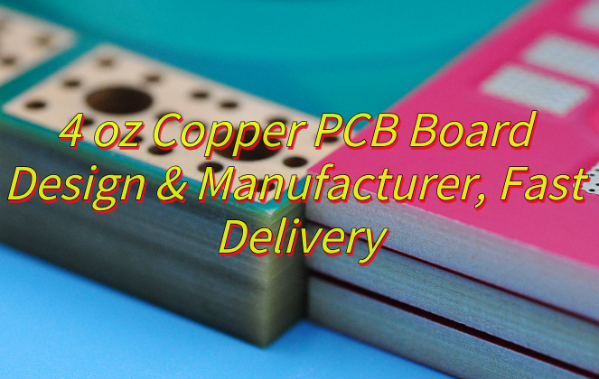
Why choose 4 oz copper PCB? This guide discover its thickness, application, design guide and spec, as well as supplier selection methods.
Are you troubled with these problems?
- How to avoid copper foil melting in high current scenarios?
- How to balance the cost and reliability of thick copper plates?
- How to efficiently achieve complex heat dissipation requirements?
EBest Circuit (Best Technology) can provide services and solutions:
- Copper thickness optimization algorithm + customized design: Based on 19 years of data accumulation, provide accurate copper thickness and line width matching solutions to ensure stability under 5A/mm² current.
- Step-by-step cost control solution: Through innovations such as local thickening and gold immersion process replacement, reduce overall costs by 15%-30% without sacrificing performance.
- Three-dimensional heat dissipation structure design: The use of embedded copper blocks and microchannel etching technology increases heat dissipation efficiency by 40%, without the need for additional heat sinks.
Welcome to contact us if you have any request for heavy copper PCB: sales@bestpcbs.com.
What Is 4 oz Copper PCB?
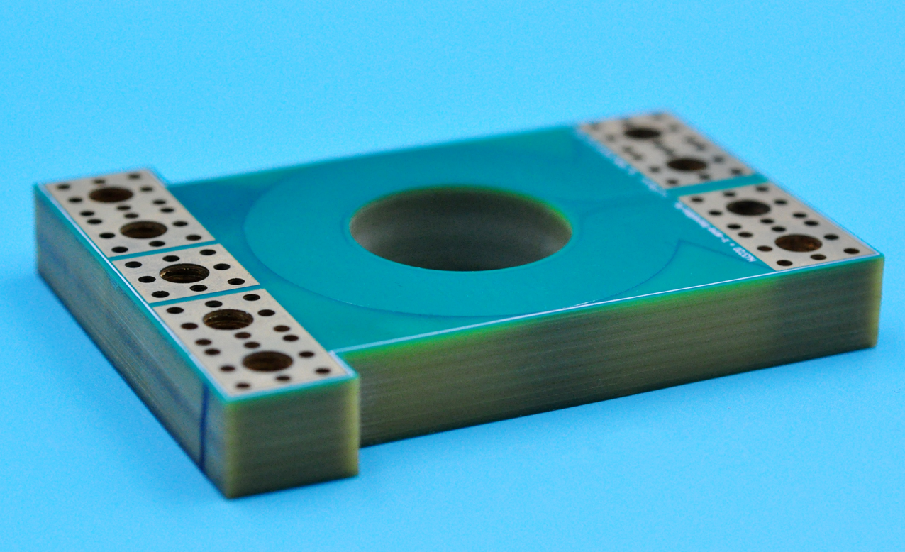
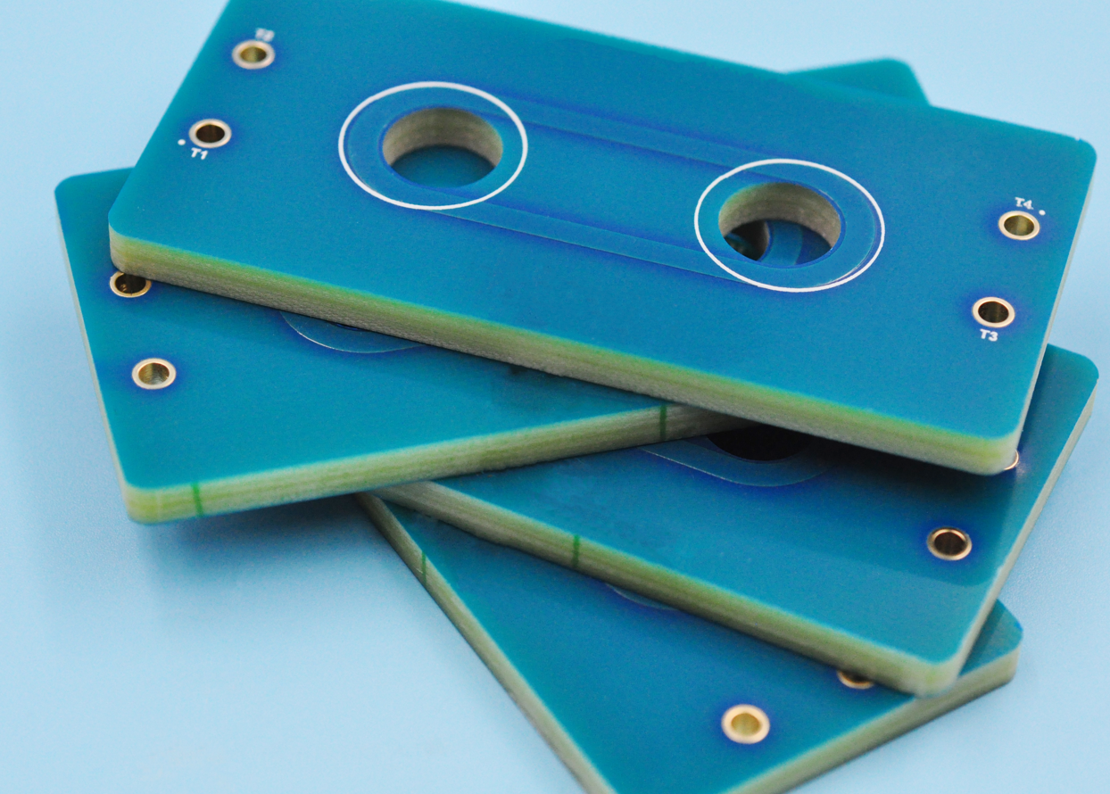
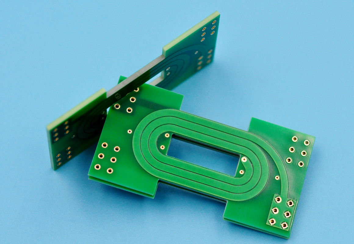
A 4 oz copper PCB refers to a printed circuit board with copper layers weighing 4 ounces per square foot, roughly 140 microns thick. This thicker copper coating allows the board to handle higher electrical currents and heat dissipation compared to standard 1 oz or 2 oz PCBs. It’s commonly used in power electronics, motor controls, automotive systems, and industrial devices where robustness and efficiency matter. Manufacturing such PCBs requires specialized techniques to ensure even copper distribution and structural integrity, making them slightly more expensive but ideal for demanding applications.
How Thick Is 4 oz of Copper PCB?
The thickness of a 4 oz copper PCB refers to the weight of copper per square foot, which translates to approximately 0.14 millimeters (mm) or 5.6 mils in physical thickness. This measurement is commonly used in printed circuit board (PCB) manufacturing to indicate the copper layer’s density, with 4 oz being a standard choice for high-current applications due to its durability and conductivity.
Why Choose 4 oz Copper PCB?
Advantages of 4 oz Copper PCB
- Enhanced Current Handling – 4 oz copper PCBs can carry higher currents without overheating, making them ideal for power electronics, motor controllers, and high-voltage systems.
- Improved Durability – The thicker copper layer resists thermal stress and mechanical wear, extending the lifespan of the PCB in demanding environments.
- Better Thermal Management – Increased copper thickness dissipates heat more efficiently, reducing the risk of component failure due to overheating.
- Reliable Signal Integrity – For high-frequency applications, the robustness of 4 oz copper minimizes signal loss and interference, ensuring stable performance.
- Cost-Effective in the Long Run – While slightly pricier than thinner alternatives, their longevity and reduced maintenance needs lower total ownership costs.
- Simplified Design Flexibility – Allows for wider traces and fewer layers, streamlining manufacturing while maintaining performance.
When to Use 4 oz Copper PCB Board?
Applications for 4 oz copper PCB board
- High-Current Power Electronics – Used in power supplies, motor controllers, and inverters to handle heavy currents efficiently.
- LED Lighting Systems – Essential for high-power LED drivers to dissipate heat and ensure stable performance.
- Automotive Electronics – Suitable for battery management systems (BMS) and EV charging circuits due to durability.
- RF and Microwave Devices – Provides low resistance for signal integrity in high-frequency applications.
- Industrial Equipment – Ideal for welding machines and robotics where robust current handling is critical.
- Solar Power Systems – Used in solar charge controllers and inverters to optimize energy conversion.
4 oz Copper PCB Design Specification
| Specification | Typical Value / Range |
| Copper Thickness | 4 oz/ft² (≈ 140 µm or 0.14 mm per layer) |
| Minimum Trace Width | ≥ 10 mil (0.254 mm) |
| Minimum Trace Spacing | ≥ 10 mil (0.254 mm) |
| Minimum Hole Diameter | 0.3 mm (can vary with board thickness) |
| Board Thickness | 1.6 mm – 3.2 mm (custom options available) |
| Max. PCB Size | Typically 600 mm × 600 mm (depends on fabrication) |
| Dielectric Material | FR4, Polyimide, or High-TG material |
| Thermal Conductivity | Depends on base material, FR4 ~0.3 W/mK, Metal Core ~1–3 W/mK |
| Surface Finish | ENIG, HASL, OSP, Immersion Silver, Immersion Tin |
| Layer Count | 1 to 12 layers (4 oz typically used in 2–6 layers) |
| Solder Mask Color | Green, Blue, Black, Red, White |
| Tg (Glass Transition Temp.) | ≥ 130°C (Standard FR4) or ≥ 170°C (High-TG) |
| Impedance Control | Optional – harder to achieve with thick copper |
| Drill Tolerance | ±0.075 mm typical |
| Aspect Ratio (Hole:Board) | ≤ 6:1 recommended for plating reliability |
How to Design A 4 oz Copper PCB Board for High Power?
4 oz copper PCB board design guide for high power application:
1. Material Selection
- Use high-Tg (≥170°C) FR4 or metal-core substrates (aluminum/copper) to withstand heat from high currents. Verify copper foil adhesion strength to prevent delamination under thermal stress.
2. Layer Stackup
- Outer layers: 4 oz copper for power/ground traces.
- Inner layers: 1-2 oz copper for signals.
- Add dedicated power/ground planes near high-current areas.
3. Trace Design
- Calculate trace width using IPC-2221 standards (e.g., 4 oz copper = ~70A for 10mm width at 10°C rise).
- Avoid sharp angles; use 45° bends to reduce impedance mismatches.
- Thicken traces near connectors/power components.
4. Thermal Management
- Fill unused areas with copper pours connected to ground/power planes.
- Place thermal vias (≥0.5mm diameter, ≥2 oz plating) under hot components to transfer heat to inner layers.
- Use metal-core bases for direct heat dissipation.
5. Power Distribution
- Split power planes for different voltage rails (e.g., 12V, 5V).
- Place decoupling capacitors close to IC power pins.
- Widen high-current paths (e.g., battery to motor) to minimize voltage drop.
6. Signal Integrity
- Keep high-speed traces (e.g., >50MHz) away from power zones.
- Adjust trace spacing to maintain 50-75Ω impedance despite thick copper.
7. Manufacturing Compliance
- Specify “4 oz copper” and “metal-core” to PCB vendors.
- Confirm minimum trace/space (≥8mil) and via drill sizes (≥0.3mm).
- Request differential etching to avoid undercutting.
8. Testing & Validation
- Perform thermal imaging under max load to identify hotspots.
- Simulate current flow with tools like PSpice or LTspice.
- Test prototype with 1.5x nominal current to validate reliability.
How to Choose A Reliable Heavy Copper PCB Manufacturer?
Methods about how to choose a reliable 4 oz copper PCB manufacturer:
- Verify Credentials & Certifications: Prioritize manufacturers with ISO 9001, UL certification, IPC compliance, and RoHS/REACH compliance.
- Assess Production Experience: Demand case studies of 4 oz copper PCB projects, especially in high-current, thermal management, or RF applications to reduces technical risks.
- Inspect Quality Control Systems: Inquire about AOI (Automated Optical Inspection), X-ray layer inspection, and electrical testing capabilities. For thick copper boards, uneven plating is a common defect, robust QC processes minimize failures.
- Evaluate Technical Expertise: Confirm the engineering team’s proficiency in impedance control, thick copper filling, and other specialized processes. Request technical whitepapers or examples of past design optimizations (Such as reducing thermal stress).
- Clarify Lead Times & Capacity: 4 oz copper PCBs require longer production cycles. Confirm if the factory has dedicated lines for thick copper boards and emergency order handling. Ask for the past 3-month on-time delivery rate (aim for ≥95%).
- Test Customer Service Responsiveness: Measure technical support reply time (ideal: ≤24 hours via email/phone). Ensure they provide DFM (Design for Manufacturability) feedback to avoid costly late-stage revisions.
- Compare Price Transparency: Request itemized quotes. Beware of hidden costs (e.g., engineering fees, testing charges). For 4 oz copper boards, reasonable price differences should stay within 15%, prioritize value over lowest bid.
- Focus on Long-Term Reliability: For high-stakes applications (e.g., industrial control, power modules), prioritize suppliers with proven defect-handling protocols. A slightly higher upfront cost often offsets project delays or field failures.
How to Get A Quote For Heavy Copper PCB Project?
All Materials Clients Need to Submit
1. Gerber Files & Drawings
- Provide complete PCB design files (including .brd, .gbl, .gtl formats), marking copper thickness distribution areas and special process requirements (e.g., stepped copper, deep copper slots).
2. Technical Specifications
- Specify:
- Copper thickness (e.g., 4oz/5.6oz)
- Layer count and stack-up structure
- Minimum trace width/spacing (≥6mil recommended for heavy copper)
- Impedance control requirements (±10% accuracy)
3. Material & Surface Finish
- Define substrate (e.g., FR4, CEM-3), solder mask color, surface treatment (HASL, ENIG, OSP), and note if high-temperature/high-TG material is needed.
4. Special Process Requirements
- Include buried/blind vias, back drilling, metal core (aluminum/copper substrate), immersion gold thickness (2-5μm recommended), with detailed design drawings.
5. Testing & Certification Needs
- List required tests: flying probe test, impedance test, thermal stress test, and third-party certifications (e.g., UL, CE).
6. Volume & Lead Time
- Provide estimated order quantity (e.g., 50pcs/500pcs) and desired delivery time, noting if split shipments are acceptable.
7. Application Description
- Briefly explain product use (e.g., new energy, automotive electronics, industrial control) to help optimize process parameters (e.g., current-carrying capacity design).
8. Contact Information
- Include company name, procurement contact, and details for smooth technical communication.
Act Now for Accurate Quotation!
EBest Circuit (Best Technology) has 19 years of expertise in heavy copper PCB manufacturing, offering 24-hour rapid prototyping. Our engineering team provides free design optimization, ensuring copper thickness uniformity within ±8% and via filling rate ≥95%. Submit materials to sales@bestpcbs.com to get a free quote now!