

What is IMS PCB?
IMS PCB stands for Insulated Metal Substrate Printed Circuit Board. It’s a specialized type of PCB designed to manage heat more effectively than standard boards. At its core, an IMS board is made of three main layers: a metal base (usually aluminum), a thermally conductive dielectric layer, and a copper circuit layer on top.
This unique construction gives IMS boards exceptional heat transfer capabilities. Unlike standard FR4 boards, where heat may accumulate and degrade performance over time, an IMS PCB actively channels heat away from components and dissipates it through the metal base. This process helps protect sensitive parts and improves overall device longevity.
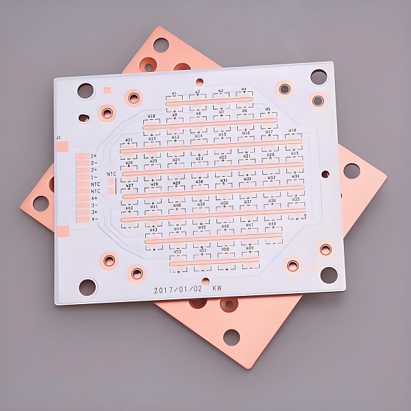
IMS PCBs are commonly used in LED lighting systems, power converters, automotive electronics, solar inverters, and industrial control systems. Any circuit that generates significant heat can benefit from the enhanced thermal management of an IMS PCB.
Features of IMS PCB
IMS PCBs are favored in demanding applications because of their distinct advantages. Below are some of the standout features:
1. The dielectric layer in an IMS PCB has much higher thermal conductivity compared to FR4.
2. Once heat reaches the metal base, it is dispersed across a larger surface area or transferred to a heatsink.
3. The metal base not only helps with heat but also strengthens the board. This added rigidity reduces the chances of warping, especially in environments with temperature cycling or mechanical stress.
4. Components perform better and last longer when they remain within optimal temperature ranges.
5. Most IMS boards are single-sided, simplifying the layout and making them easier to manufacture. However, advanced designs may include multilayer configurations when required.
6. The metal base can also serve as a shield against EMI interference, which is useful in sensitive analog or RF applications.
Types of IMS Boards
Different IMS boards are used for different applications depending on the metal type and overall construction. Here are the three primary types:
- Aluminum-Based IMS PCB
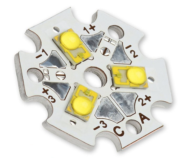
This is the most popular type and often the first choice for LED lighting and consumer electronics. Aluminum is lightweight, affordable, and has decent thermal performance. It strikes a balance between cost and functionality for a wide range of applications.
- Copper-Based IMS PCB
Copper has better thermal and electrical conductivity than aluminum. These boards are used in high-end applications where superior thermal management is critical, such as power modules, solar inverters, and automotive control systems. However, copper is more expensive and heavier than aluminum.
- Steel-Based IMS PCB
Less common but useful in environments where mechanical durability is crucial. Steel doesn’t conduct heat as efficiently as copper or aluminum but provides maximum rigidity and resistance to deformation. It’s mainly used in industrial or military electronics.
Each type of IMS PCB is selected based on the specific needs of your project. Aluminum offers a good starting point, copper pushes performance higher, and steel provides strength for the harshest conditions.
IMS PCB Stack-up
A critical element in IMS board design is the stack-up, which refers to how the different layers of the board are arranged. The typical IMS PCB stack-up includes the following:
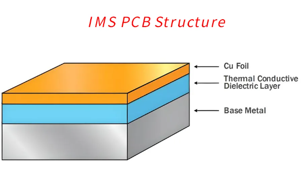
1. Copper Layer
This is where all the electronic traces and pads are formed. The copper thickness usually ranges from 1 oz to 3 oz per square foot, depending on current requirements. It serves as the pathway for electrical signals and power.
2. Dielectric Layer
This is the thermally conductive but electrically insulating layer that separates the copper and the metal base. It’s usually made of a polymer filled with ceramic particles. The dielectric plays a vital role in transferring heat efficiently while preventing short circuits. The thickness typically ranges from 0.075 mm to 0.2 mm, with thermal conductivity from 1 to 7 W/m·K, depending on material grade.
3. Metal Base
This is typically made of aluminum, copper, or steel. The metal provides mechanical support and acts as the main heat dissipation path. Its thickness usually ranges from 1 mm to 2 mm, but thicker bases are used in heavy-duty applications.
Some advanced designs may include additional dielectric and copper layers to create double-layer or multilayer IMS PCBs, though this increases cost and complexity.
How Thick is an IMS PCB?
The total thickness of an IMS PCB is influenced by the materials used and application requirements. On average, the board thickness ranges from 0.8 mm to 3.2 mm, but custom configurations are available.
Here’s a breakdown of each layer’s contribution to overall thickness:
- Copper Layer: 35–105 µm (1–3 oz)
- Dielectric Layer: 75–200 µm
- Metal Base Layer: 1.0–2.0 mm (for aluminum or copper)
Applications requiring high current typically demand thicker copper layers and sometimes thicker base metals. Likewise, if better insulation is needed, the dielectric layer can be made thicker, but this may reduce heat transfer efficiency. Engineers must balance electrical, thermal, and mechanical requirements to define the most suitable thickness.
What is the Difference Between IMS PCB and FR4 PCB?
Though both are used in electronic devices, the differences between IMS PCB and FR4 PCB are quite substantial:
| Parameter | IMS PCB | FR4 PCB |
| Full Name | Insulated Metal Substrate PCB | Flame Retardant Grade 4 PCB |
| Base Material | Metal core (usually aluminum or copper) | Fiberglass-reinforced epoxy (FR4) |
| Thermal Conductivity | High (1–7 W/m·K, depending on dielectric) | Low (typically 0.3–0.4 W/m·K) |
| Heat Dissipation | Excellent, through metal base | Limited, requires heatsinks or fans |
| Layer Structure | Usually single-sided | Can be single, double, or multilayer |
| Mechanical Strength | High (due to metal base) | Moderate (flexible but less rigid) |
| Weight | Heavier (due to metal core) | Lighter |
| Manufacturing Cost | Higher | Lower |
| Applications | Power electronics, LEDs, automotive, solar | Consumer electronics, IoT, communication devices |
| Thermal Resistance | Low (better heat flow) | High (poor thermal path) |
| Electrical Insulation | Through thermally conductive dielectric | Provided by FR4 material itself |
| Common Copper Thickness | 1–3 oz | 1–2 oz |
| Typical Board Thickness | 0.8–3.2 mm | 0.6–2.0 mm |
| Design Complexity | Lower (usually single-layer) | Higher (multilayer and complex routing possible) |
| Price Range | Mid to High | Low to Mid |
What is the Thermal Resistance of IMS Board?
Thermal resistance (Rθ) refers to a material’s resistance to heat flow. In IMS PCBs, it is mainly influenced by the dielectric layer. A lower Rθ means better heat transfer and lower temperature rise.
The thermal resistance of an IMS board is calculated using:
Rθ = t / (k × A)
Where:
t = dielectric thickness
k = thermal conductivity
A = surface area
Typical values for IMS PCBs range from 0.2°C/W to 1.0°C/W, depending on materials and layout. Advanced dielectric materials with high k-values can push this number lower, helping improve performance in high-power applications.
Designers often select materials with k ≥ 3 W/m·K and limit the dielectric layer to under 150 µm to achieve low thermal resistance.
EBest Circuit (Best Technology) – Reliable IMS PCB Manufacturer
If you’re sourcing IMS PCBs and want consistent quality, EBest Circuit (Best Technology) is your go-to IMS PCB manufacturer. We have a dedicated production line for metal-core PCBs, including aluminum, copper, and hybrid metal boards.
Why Choose EBest Circuit (Best Technology)?
✅ Professional Engineering Support: Our experienced team helps optimize stackups, select dielectric materials, and improve thermal paths in your layout.
✅ ISO Certifications: We are certified with ISO9001, IATF16949, ISO13485, and AS9100D, serving a wide range of industries including medical, automotive, and aerospace.
✅ MES Traceability: Every board is tracked using our MES system to ensure complete traceability from raw materials to final shipment.
✅ Flexible Volumes: Whether you need a prototype batch or full-scale production, we offer scalable solutions.
✅ Comprehensive IMS PCB Assembly: Beyond PCB fabrication, we also offer full assembly including component sourcing, reflow soldering, inspection, and testing.
From concept to finished product, we work closely with clients to deliver high-performance IMS PCBs that meet electrical, mechanical, and thermal demands.
FAQs
1. What does IMS PCB stand for?
It stands for Insulated Metal Substrate Printed Circuit Board, a high-performance board for heat-sensitive applications.
2. Can IMS PCB be double-sided?
Yes, though less common. Double-sided IMS PCBs require more advanced fabrication and cost more, but they’re available for complex designs.
3. Is IMS PCB good for automotive systems?
Absolutely. Automotive systems generate a lot of heat and require reliability. IMS PCBs are ideal for ECUs, power converters, and headlight controls.
4. What thermal conductivity should I choose for my dielectric layer?
It depends on the heat generated. For moderate power, 1–2 W/m·K is enough. For high-power LEDs or power modules, choose ≥3 W/m·K.
5. How do I request a quote from EBest Circuit (Best Technology)?
Send your Gerber files, stackup requirements, and assembly needs to our team, and we’ll respond with a customized quote within 24 hours.
Tags: Ims pcb assembly, Ims pcb definition, Ims pcb manufacturer