

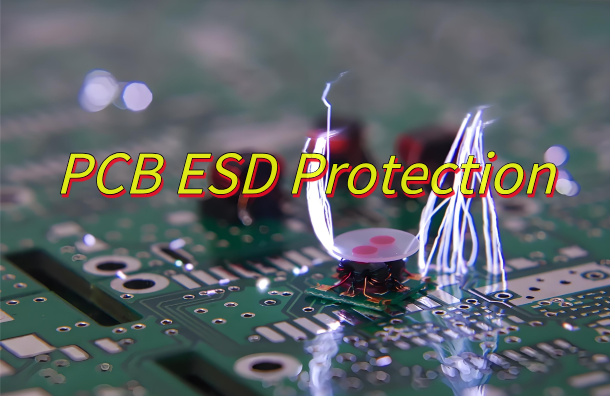
What is PCB ESD protection? This guide explores standards, design strategies, implementation methods, and verification processes for comprehensive ESD protection.
EBest Circuit (Best Technology) delivers comprehensive PCB ESD protection solutions backed by 18 years of industry expertise. Our certified engineers design multilayer boards with optimized grounding strategies, proper component spacing, and advanced transient voltage suppressors to meet IEC 61000-4-2 Level 4 standards. We implement cutting-edge techniques including guard rings, spark gaps, and ESD-resistant materials while maintaining cost efficiency. From medical devices to automotive electronics, our solutions prevent latent failures through rigorous HBM/CDM testing. Clients benefit from our full-service capabilities from schematic review to final compliance testing, ensuring robust ESD protection without compromising signal integrity. Contact our team for tailored solutions that enhance reliability while reducing development cycles: sales@bestpcbs.com.
What Is PCB ESD Protection?
PCB ESD Protection refers to the systematic approach of designing printed circuit boards to safely manage electrostatic discharge (ESD) events. Fundamentally, it involves creating controlled pathways that divert potentially damaging electrical surges away from sensitive components before they can cause harm. This protection is achieved through careful board layout, strategic component placement, and intentional routing techniques that collectively absorb or redirect sudden voltage spikes.
Consequently, effective PCB ESD Protection integrates multiple design elements: dedicated transient suppressors near entry points, optimized grounding structures with low-impedance paths to earth, and physical isolation of high-risk circuits. Additionally, techniques like guard rings around connectors, minimized trace lengths near board edges, and avoidance of floating metal planes contribute significantly. By implementing these measures, designers establish a robust defense against ESD-induced failures such as latch-up, gate oxide damage, or data corruption, ultimately enhancing product durability and field reliability.
ESD PCB Protection Standards
Here are standards for ESD PCB protection:
- IEC 61000-4-2: Defines test methods for immunity to electrostatic discharge, specifying voltage levels (e.g., ±2kV–±15kV) and waveform parameters. Widely adopted for consumer and industrial electronics, it guides PCB layout and component selection to withstand direct contact or air discharges.
- ANSI/ESD S20.20: Focuses on electrostatic control programs for manufacturing environments. While not PCB-specific, it mandates grounding requirements and material handling protocols that influence board design, such as avoiding charge accumulation on unconnected traces.
- IPC-A-610: Outlines acceptability criteria for assembled PCBs, including ESD-related defects like damaged pads or components. Helps ensure protection measures (e.g., TVS diode soldering quality) meet reliability thresholds during production.
- ISO 10605 (Automotive): Addresses ESD robustness for vehicles, emphasizing higher immunity levels (±25kV) due to harsh operating conditions. PCB designs must incorporate enhanced shielding and redundant grounding for sensors and infotainment systems.
- MIL-STD-883 (Method 3015): Military-grade standard requiring rigorous ESD testing for mission-critical hardware. Demands multilayer boards with isolated power planes and minimized loop areas to prevent coupling.
- EN 61340-5-1: Covers electrostatic protection for electronic devices, stressing the importance of static-dissipative materials in PCB substrates and enclosures to reduce charge generation.
What Are Strategies for PCB ESD Protection Design?
Here are practical PCB ESD protection design strategies with specific implementation details:
Component Selection and Strategic Positioning
- ESD-Rated Components: Integrate devices with inherent ESD robustness, such as TVS diodes, Zener diodes, or ESD suppressors, particularly for exposed interfaces (e.g., USB, Ethernet, SD cards).
- Placement Priorities: Position ESD protection components near connectors or entry points to intercept discharges before they reach sensitive circuitry. Keep vulnerable ICs (e.g., microcontrollers, amplifiers) away from board edges.
- Shielding Techniques: Use metal can shields or conductive enclosures for components susceptible to indirect ESD fields.
Grounding and Power Integrity
- Unified Ground Plane: Design a solid ground plane to minimize impedance and provide a direct path for ESD currents. Avoid ground plane segmentation unless necessary for signal isolation.
- Multi-Point Grounding: Connect chassis and PCB grounds at multiple strategic locations to reduce inductive loops
- Decoupling Networks: Place high-frequency ceramic capacitors (e.g., 0.1µF X7R) close to power pins of ICs. Add bulk capacitors (e.g., 22µF–100µF) at power entry points to filter low-frequency noise.
Trace and Layer Design
- Minimize Trace Length: Route high-speed signals and ESD-sensitive traces as short as possible to reduce inductive coupling risks.
- Avoid Parallel Routing: Offset high-speed data lines from ESD-prone traces (e.g., reset lines) to prevent crosstalk.
- Layer Stackup: Use a 4-layer or 6-layer PCB with dedicated ground/power planes. Position signal layers adjacent to ground planes for improved shielding.
Protection Circuit Integration
- TVS Diode Arrays: Deploy bidirectional TVS diodes at interface points to clamp ESD voltages below device thresholds. Select diodes with fast response times (<1 ns) and low leakage.
- Series Termination Resistors: Insert 10Ω–47Ω resistors in series with signal lines to limit ESD current without degrading signal quality.
- Filter Networks: Implement RC filters (e.g., 1kΩ resistor + 1nF capacitor) for low-speed signals to attenuate high-frequency ESD transients.
Mechanical and Coating Solutions
- Guard Rings: Surround sensitive analog circuits with grounded copper rings to intercept stray ESD currents.
- Conformal Coating: Apply protective coatings (e.g., acrylic, silicone) to exposed PCB areas to prevent direct discharge.
- Metallic Enclosures: Use EMI gaskets and conductive foam for enclosures to block external ESD fields.
Considerations in PCB ESD Protection Design
Below are considerations in PCB ESD protection design:
- Component Selection: Choose ESD-suppression devices like TVS diodes or Zener clamps tailored to interface voltages, placing them near connectors to intercept discharges early. Pair with series resistors (10–47Ω) and decoupling capacitors (0.1µF–10µF) to limit current spikes and stabilize power rails.
- Layout Optimization: Isolate sensitive circuitry from board edges and high-risk zones. Shorten traces for high-speed signals and critical nodes to reduce inductive coupling. Use grounded copper guard rings around analog sections and low-impedance ground planes with multi-point chassis connections to minimize loops.
- Protection Circuits: Integrate bidirectional TVS diode arrays at interface points for voltage clamping. Implement RC filters (1kΩ + 1nF) for low-speed signals and ferrite beads for noise suppression. Avoid parallel routing of high-speed and ESD-prone traces.
- Mechanical Safeguards: Apply conformal coatings (e.g., acrylic, silicone) to exposed PCB areas. Use metallic shields or EMI gaskets for enclosures to block external ESD fields. Secure cable shields to chassis grounds at both ends.
- Testing and Validation: Conduct IEC 61000-4-2 compliance testing (±8kV contact/±15kV air) using calibrated ESD simulators. Analyze waveform captures to refine clamping thresholds and component placements. Iterate designs based on failure modes.
- Material and Fabrication: Select PCB materials with moderate dielectric constants (e.g., FR-4) and controlled impedance for high-speed signals. Enforce ESD-safe assembly practices, including humidity control, ionization, and grounded workstations.
- System-Level Measures: Use optocouplers or digital isolators for harsh ESD environments. Implement error-correcting codes (e.g., CRC) and watchdog timers in firmware to tolerate transient faults. Design shielded cabling with proper drain wires.
How to Protect PCB from ESD?
Practical strategies for reliability and cost savings:
Use ESD-Rated Components at Entry Points
- Install transient voltage suppression (TVS) diodes or Zener clamps near connectors, buttons, and antennas to intercept ESD before it reaches sensitive chips.
- Why: Reduces component damage, lowers repair costs, and prevents unexpected field failures.
Optimize PCB Layout for Shortest Paths
- Keep high-speed signals and ESD-sensitive traces short and away from board edges. Route power/ground planes continuously to avoid loops.
- Why: Minimizes inductive coupling and signal distortion, ensuring stable performance and fewer customer complaints.
Add Layered Protection Circuits
- Combine TVS diodes with series resistors (10–47Ω) and decoupling capacitors (0.1µF ceramic + 10µF electrolytic) to filter high-frequency noise and limit current spikes.
- Why: Improves immunity to discharges, extending product lifespan and reducing warranty claims.
Isolate Sensitive Areas with Guard Rings
- Surround analog circuits, oscillators, and low-power ICs with grounded copper rings to block stray ESD currents.
- Why: Prevents false triggers and data corruption, enhancing user experience and brand reputation.
Apply Mechanical Shielding and Coatings
- Use conformal coatings (e.g., acrylic, silicone) on exposed PCB areas and metallic shields for enclosures to block external ESD fields.
- Why: Protects against direct discharges in harsh environments, such as industrial or outdoor settings.
Validate with IEC 61000-4-2 Testing
- Test prototypes using calibrated ESD simulators (±8kV contact, ±15kV air) and refine designs based on waveform analysis.
- Why: Ensures compliance with global standards, avoiding costly redesigns and market entry delays.
Collaborate with Manufacturers for ESD-Safe Assembly
- Enforce ESD control procedures during PCB assembly, including humidity-controlled environments, ionized air blowers, and grounded workstations.
- Why: Prevents damage during production, reducing scrap rates and maintaining on-time deliveries.
Design System-Level Resilience
- Use shielded cables for external connections, isolate interfaces with optocouplers, and embed error-correcting firmware (e.g., CRC checks).
- Why: Tolerates transient faults without performance degradation, boosting customer satisfaction and loyalty.
How to Add ESD Protection to PCB?
Practical steps for enhanced durability and cost efficiency:
1. Start with ESD-Rated Components at Vulnerable Points
- Place TVS diodes, Zener clamps, or polymer ESD suppressors directly at connectors, switches, and antennas, common entry points for ESD.
- Benefit: Prevents costly component replacements and field failures by neutralizing discharges before they harm sensitive chips.
2. Optimize Trace Routing and Layer Design
- Keep high-speed signal traces short and away from board edges. Use a solid ground plane with minimal splits to reduce inductive loops.
- Benefit: Lowers signal interference and product returns due to unpredictable behavior.
3. Layer Protection with Resistors and Capacitors
- Add 10–47Ω series resistors to limit ESD current and 0.1µF ceramic capacitors to filter high-frequency noise. Combine with ferrite beads for additional suppression.
- Benefit: Extends product lifespan and reduces warranty costs by mitigating voltage spikes.
4. Isolate Sensitive Circuits with Guard Rings
- Surround analog components, oscillators, and low-power ICs with grounded copper rings to block stray ESD currents.
- Benefit: Maintains precision performance and avoids data corruption, enhancing user trust.
5. Incorporate Mechanical Shielding
- Apply conformal coatings (e.g., acrylic, silicone) to exposed PCB areas and use metallic shields for enclosures in high-risk environments.
- Benefit: Ensures reliability in industrial or outdoor settings, reducing replacement needs.
6. Validate Designs with Rigorous Testing
- Perform IEC 61000-4-2 compliance tests (±8kV contact, ±15kV air) using ESD simulators. Refine designs based on waveform analysis.
- Benefit: Avoids costly redesigns and delays by addressing ESD issues early.
7. Collaborate with Manufacturers for ESD-Safe Production
- Enforce ESD control during assembly: use humidity-controlled rooms, ionized air, and grounded tools.
- Benefit: Minimizes production scrap and ensures on-time delivery without quality compromises.
8. Design for System-Level Resilience
- Use shielded cables, optocouplers for noisy interfaces, and error-correcting firmware (e.g., CRC checks) to tolerate transient faults.
- Client benefit: Delivers a robust product that performs reliably in diverse conditions, boosting customer loyalty.
How to Achieve ESD Protection via PCB Trace?
Optimize Trace Width and Spacing
- Use wider traces (≥0.3mm) for power/ground networks to lower resistance and improve ESD current handling. Maintain ≥0.2mm spacing between traces to prevent accidental arc-over during discharges.
- Why: Reduces thermal stress and trace damage, cutting repair costs and downtime.
Shorten Sensitive Signal Paths
- Route high-speed data lines, reset pins, and analog circuits as close to ground planes as possible. Avoid looping or meandering traces to minimize inductive coupling risks.
- Why: Prevents signal corruption and false triggers, ensuring consistent performance in the field.
Prioritize Solid Ground Planes
- Design unbroken ground layers on inner PCB layers to create a low-impedance path for ESD currents. Avoid splitting grounds unless absolutely necessary for noise isolation.
- Why: Distributes ESD energy evenly, preventing localized voltage spikes that could fry components.
Strengthen Layer Connections with Stitching Vias
- Place multiple vias (≥0.3mm diameter) between ground planes and outer layers near connectors. This reduces loop inductance and improves ESD current dissipation.
- Why: Enhances protection against high-voltage spikes, safeguarding nearby components.
Keep Traces Away from PCB Edges
- Position critical traces at least 2mm from board edges to shield them from external ESD fields. Use inner layers for ultra-sensitive signals if space allows.
- Why: Reduces exposure to direct discharges during handling or assembly, extending product life.
Guard Sensitive Signals with Copper Rings
- Add grounded copper traces alongside differential pairs or low-voltage analog lines to block ESD interference. Connect guards to ground at both ends for maximum effect.
- Why: Maintains signal clarity in noisy environments, preventing data errors and system crashes.
Add Localized Decoupling Near Power Pins
- Place 0.1µF ceramic capacitors within 2mm of IC power pins to filter ESD-induced noise. Pair with 10µF bulk capacitors at the board level for comprehensive power stabilization.
- Why: Stabilizes power rails during ESD events, avoiding microcontroller resets and memory glitches.
How to Verify the PCB ESD Protection Effect?
Below are measures about how to verify the PCB ESD protection effect:
Conduct IEC 61000-4-2 Compliance Testing
- Use a calibrated ESD simulator to apply controlled discharges (±8kV contact, ±15kV air) to connectors, buttons, and seams. Monitor the PCB for functional failures, resets, or component damage.
- Why: Validates compliance with global standards, reducing market entry barriers and liability risks.
Perform Real-World Stress Tests
- Simulate human-body discharges (e.g., 4kV for desktop devices, 8kV for industrial gear) using a discharge network. Test under operational conditions to uncover hidden vulnerabilities.
- Why: Identifies weaknesses in sensitive areas like reset pins or communication interfaces.
Analyze Waveform Captures
- Use an oscilloscope with high-voltage probes to measure ESD current and voltage waveforms at key nodes (e.g., TVS diode clamps, power rails). Compare results against component datasheet limits.
- Why: Reveals overshoot or ringing that could degrade long-term reliability.
Inspect for Physical Damage
- Examine PCB traces, capacitors, and ICs under a microscope post-testing. Look for solder joint cracks, delamination, or charred components.
- Why: Prevents latent failures that could surface after deployment.
Validate Power Integrity During Discharge
- Monitor power rails (e.g., 3.3V, 5V) with a differential probe during ESD events. Ensure voltage drops stay within 10% of nominal levels to avoid microcontroller resets.
- Why: Maintains system stability and prevents data corruption.
Test System-Level Resilience
- Evaluate end-to-end functionality (e.g., communication protocols, user interfaces) during and after ESD pulses. Check for false triggers, lockups, or performance degradation.
- Why: Ensures a seamless user experience and minimizes field returns.
Document and Iterate
- Generate a detailed test report including setup photos, waveform screenshots, and failure analysis. Use findings to refine component placement, trace routing, or protection circuits.
- Why: Creates a feedback loop for continuous improvement, reducing future redesign costs.
Conclusion
Effective PCB ESD protection requires multi-layered approaches from component selection to layout design and rigorous testing. Main strategies include proper grounding, transient voltage suppressors, and careful trace routing. Standards vary by application, with industrial/automotive requiring higher protection levels than consumer electronics. Implementation demands attention to connector design, board edge protection, and material selection. Verification should include both contact and air discharge testing at progressively higher voltages. For optimized ESD protection solutions tailored to your specific requirements, contact EBest Circuit (Best Technology) for professional consultation and competitive pricing. Our expertise can help prevent costly field failures while meeting all compliance standards: sales@bestpcbs.com.
Tags: PCB ESD Protection