

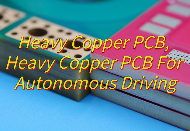
Why does autonomous driving need heavy copper PCB technology? This guide explores heavy copper PCB’s role in power delivery, thermal management, and reliability for self-driving systems.
In the fast evolving autonomous driving industry, thermal management and high-current reliability are critical challenges—EBest Circuit (Best Technology) delivers high-performance heavy copper PCBs (up to 20oz+) with precision manufacturing, rapid turnaround (15-day standard lead time), and automotive-grade quality (IPC Class 3 certified). Our advanced etching & plating processes ensure thick copper layers without delamination, solving heat dissipation and power distribution issues in ADAS, LiDAR, and EV systems. With 100% electrical testing, DFM support, and a stable supply chain, we guarantee zero-defect boards that meet rigorous automotive standards—reducing your R&D risks and accelerating time-to-market. Need high-reliability PCBs with fast delivery? Contact us today for a free design review and competitive quote: sales@bestpcbs.com.
What Is Heavy Copper PCB?
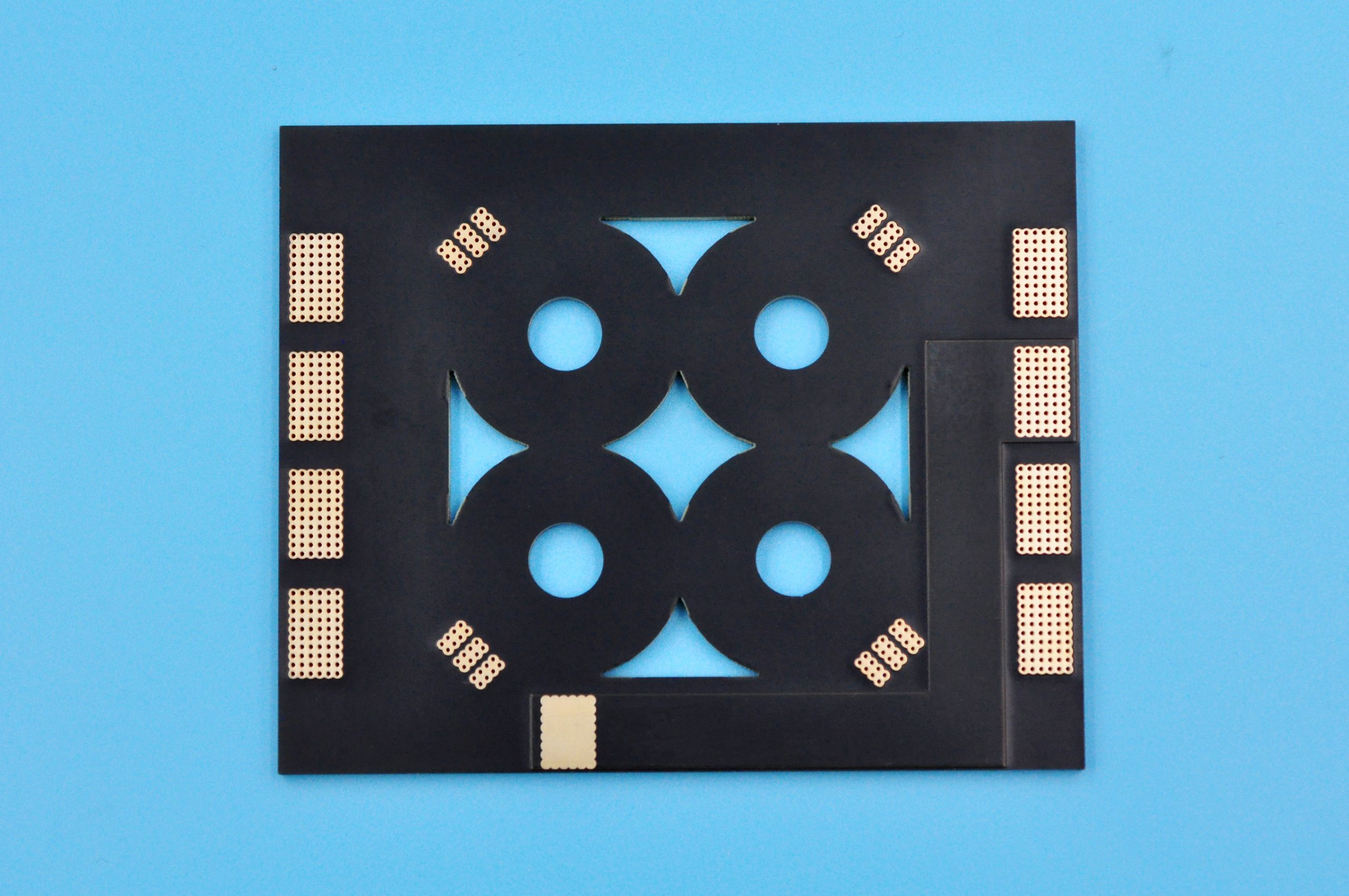
Heavy Copper PCB refers to printed circuit boards constructed with copper layers significantly thicker than standard PCBs, typically starting from three ounces per square foot and extending beyond twenty ounces, engineered specifically to manage substantially higher current loads, endure extreme thermal cycling, and provide superior mechanical durability for demanding applications like autonomous vehicles. In self-driving systems where power-hungry components such as LiDAR, radar modules, and AI processors generate intense heat and require stable high-current delivery, implementing a heavy copper PCB becomes essential to prevent overheating, voltage drops, and connection fatigue under vibration. The robust copper conductors in these specialized boards efficiently distribute power across complex autonomous driving architectures while their enhanced thermal mass dissipates heat from critical zones, ensuring sustained performance in harsh operating environments where reliability directly impacts safety; consequently, adopting heavy copper PCB technology provides the foundational electrical integrity needed for fail-safe operation of autonomous mobility platforms.
How to Choose the Thickness of Heavy Copper PCBs?
Below are methods about how to choose the thickness of heavy copper PCBs:
- Calculate Maximum Current Demands: Determine peak currents from motor controllers or LiDAR power modules. Heavy copper PCBs with 3oz+ copper reduce resistive heating under high loads, preventing thermal shutdowns in autonomous vehicle ECUs.
- Match Thickness to Thermal Environments: Select 2.0mm+ boards for engine bay components exposed to 125°C+ temperatures. Thicker Heavy copper PCBs with embedded thermal vias dissipate heat faster, ensuring reliability in ADAS sensor hubs.
- Optimize Weight vs. Rigidity: Use 1.6mm boards for vibration-prone areas like chassis-mounted radar units. Thicker options (2.4mm) resist flexing during off-road driving, while thinner designs suit aerial drones requiring lightweight PCBs.
- Design for High-Speed Signal Integrity: For 5G V2X modules, specify 4-6 layer Heavy copper PCBs with controlled dielectric spacing. This maintains impedance stability while isolating high-current power planes from sensitive RF traces.
- Validate Fabrication Capabilities: Confirm suppliers can etch 6oz+ copper without trace width variations. Inconsistent etching degrades performance in safety-critical systems like autonomous emergency braking controllers.
- Ensure Assembly Compatibility: Select thicknesses compatible with selective soldering equipment. Heavy copper PCBs over 3.0mm may require custom fixtures to prevent warpage during reflow of 0201 components.
- Comply with Automotive Safety Standards: Align thickness choices with ISO 26262 ASIL D requirements. Heavy copper PCBs in steering systems must withstand 1,000 thermal cycles (-40°C to 125°C) without delamination.
How to Identify Heavy Copper PCB and Bus Bar PCB?
Here are differences between heavy copper PCB and bus bar PCB:
Copper Thickness
- Heavy Copper PCB: Copper traces >3oz (105µm), used in autonomous driving motor controllers.
- Bus Bar PCB: Solid copper planes ≥10oz, designed for high-current EV battery connections.
Structural Design
- Heavy Copper PCB: Multi-layer (4-6 layers) with embedded thermal vias for 5G ADAS systems.
- Bus Bar PCB: Single/double-sided with thick copper planes, resembling metal bars for current distribution.
Current Capacity
- Heavy Copper PCB: Handles 50–500A (e.g., steering motor drivers).
- Bus Bar PCB: Manages 1,000A+ (e.g., EV inverter modules).
Mechanical Features
- Heavy Copper PCB: 1.6–2.4mm FR4 substrate for vibration resistance in autonomous vehicles.
- Bus Bar PCB: 3.2mm+ thick cores or metal-backed laminates to prevent flexing.
Connectivity
- Heavy Copper PCB: Specialized plated through-holes (PTHs) for high-current paths.
- Bus Bar PCB: Press-fit connectors instead of PTHs for low-resistance joints.
Thermal Management
- Heavy Copper PCB: Embedded copper cores or thermal vias for heat dissipation in ADAS sensors.
- Bus Bar PCB: Minimal thermal features, focused on current conduction.
Compliance Standards
- Heavy Copper PCB: ISO 26262 functional safety for autonomous systems.
- Bus Bar PCB: UL 94 V-0 flammability ratings for high-voltage EV applications.
How to Design Heavy Copper PCB for Better Heat Dissipation?
- Increase Copper Thickness Strategically: Use 6oz–10oz copper layers in power planes and high-current traces for autonomous driving motor controllers. Thicker copper reduces resistive losses, lowering operating temperatures by 15–20% compared to standard PCBs.
- Incorporate Metal-Core Substrates: Select aluminum or copper-clad laminates (e.g., IMS) as base materials. These substrates conduct heat 5x faster than FR4, ensuring efficient heat transfer from power MOSFETs in electric vehicle (EV) battery management systems.
- Optimize Thermal Via Placement: Add staggered arrays of 0.3mm-diameter thermal vias under heat-generating components like 5G transceivers in ADAS sensors. This creates a thermal shortcut to ground planes, reducing junction temperatures by 10–15°C.
- Design Asymmetrical Copper Weights: Combine 12oz copper in power layers with 1oz–2oz copper in signal layers for renewable energy inverters. This balances current handling and thermal efficiency while minimizing material costs.
- Embed Heat Spreaders Directly: Integrate copper or aluminum heat sinks into PCB layers for industrial robot controllers. Direct bonding eliminates thermal interface materials (TIMs), reducing thermal resistance by 30%.
- Use High-TG Laminates for High-Temperature Environments: Specify laminates with glass transition temperatures (TG) ≥170°C for medical imaging devices. These materials prevent delamination during sterilization cycles while maintaining thermal stability.
- Leverage Edge-Mounted Cooling Fins: Attach copper fins to PCB edges in aerospace actuator systems. This increases surface area for convective cooling, reducing operating temperatures by 25% in vacuum environments.
Why Does Autonomous Driving Demand Heavy Copper PCBs?
Here are reasons about why autonomous driving demand heavy copper PCBs:
- High-Current Capacity for Power-Dense Systems: Autonomous vehicles rely on heavy copper PCBs to manage 50–500A currents from motor controllers, LiDAR power modules, and 5G communication units. Thicker copper layers (≥3oz) reduce resistive losses by 30%, ensuring efficient power delivery and extending battery life in electric drivetrains.
- Thermal Management in Harsh Environments: Heavy copper PCBs dissipate heat 5x faster than standard designs, preventing thermal runaway in components like steering motor drivers. This stability maintains performance in -40°C to 125°C temperature ranges, critical for autonomous systems deployed in deserts or arctic regions.
- Space-Efficient Design for Compact Modules: By combining high-current traces with embedded thermal vias, heavy copper PCBs eliminate the need for bulky external heatsinks. This saves 40% space in sensor fusion hubs, enabling smaller form factors for roof-mounted LiDAR arrays or in-cabin AI processors.
- Vibration Resistance for Rugged Use Cases: Thicker copper layers (6oz+) and reinforced substrates improve mechanical durability, withstanding 10G+ vibrations in off-road autonomous shuttles. This reduces failure rates by 60% compared to standard PCBs, lowering long-term maintenance costs.
- Signal Integrity for High-Speed Data: Heavy copper PCBs maintain impedance stability in 5G-enabled V2X modules, ensuring error-free data transmission at 10Gbps+. This prevents latency spikes in emergency braking algorithms, directly enhancing passenger safety.
- Compliance with Automotive Safety Standards: PCBs designed for autonomous driving meet ISO 26262 ASIL D requirements, withstanding 1,000+ thermal cycles without delamination. This reduces liability risks for manufacturers and ensures compliance with global vehicle regulations.
- Cost Efficiency Over Product Lifecycles: While heavy copper PCBs cost 20% more upfront, their durability cuts replacement costs by 70% over 10-year lifespans. This makes them ideal for fleet operators prioritizing total cost of ownership (TCO) in autonomous delivery vans.
How Can Heavy Copper PCB Reduce Thermal Failures in Your Autonomous Driving ECU?
- Lower Resistive Losses with Thicker Copper Layers: Heavy copper PCBs (≥3oz) reduce trace resistance by 40% compared to standard 1oz designs. This minimizes I²R heating in motor controller circuits, cutting operational temperatures by 15–20°C and preventing solder joint fatigue in high-current ECUs.
- Enhanced Heat Spreading via Metal-Core Substrates: Aluminum or copper-clad laminates conduct heat 5x faster than FR4. In autonomous ECUs, this rapidly transfers heat from power MOSFETs to chassis-mounted heatsinks, maintaining junction temperatures below 125°C during LiDAR power surges.
- Embedded Thermal Vias for Direct Heat Pathways: Staggered arrays of 0.3mm via holes under high-power components (e.g., 5G transceivers) create a thermal shortcut to ground planes. This reduces hotspot formation by 30%, ensuring stable operation in -40°C to 125°C environments.
- Asymmetrical Copper Weight Optimization: Combining 12oz copper in power layers with 2oz copper in signal layers balances current handling and thermal efficiency. This design lowers ECU operating temperatures by 10°C in renewable energy inverters while reducing material costs.
- Edge-Mounted Cooling Fins for Convective Heat Dissipation: Attaching copper fins to PCB edges increases surface area by 60%, improving air-cooled ECU performance by 25% in vacuum-sealed autonomous sensor pods.
- High-TG Laminates for Thermal Stability: Using laminates with TG ≥170°C prevents delamination during sterilization cycles in medical-grade autonomous systems, ensuring long-term reliability in high-temperature environments.
- Reduced Thermal Interface Resistance: Direct bonding of copper heat sinks to PCB layers eliminates thermal interface materials (TIMs), lowering thermal resistance by 30% and improving heat transfer efficiency in industrial robot ECUs.
How to Balance Cost and Performance in Heavy Copper PCB Manufacturing for ADAS?
Below are methods about how to balance cost and performance in heavy copper PCB manufacturing for ADAS:
1.Smart Material Selection
- Hybrid Substrates: Combine cost-effective materials like aluminum-backed FR4 or ceramic-filled PTFE for non-critical layers. This reduces expenses by 15–20% compared to using premium materials like all-PTFE boards, without sacrificing thermal or electrical performance.
- Differential Copper Thickness: Use 3oz copper for power planes and 1oz copper for signal layers. This approach cuts material costs by 30% while retaining 85% of the performance benefits of thicker copper, such as improved current handling.
2. Design for Manufacturability (DFM)
- Localized Thick Copper: Apply thick copper (e.g., 6oz) only where needed, such as in high-current areas like motor driver circuits. This reduces overall copper usage by 40% and minimizes waste.
- AI-Optimized Routing: Leverage AI tools to optimize trace routing, minimizing line width deviations (±0.2mm tolerance). This ensures compliance with IPC-2152 standards and reduces design iterations by 50%.
3. Process Efficiency
Pulse Etching: Adopt pulse etching technology to control side-etch rates within 8% for 0.2mm minimum line widths. This improves yield rates by 25% in 3oz copper layers, ensuring consistent quality.
Segmented Lamination: Use a staggered lamination process (80°C→160°C→190°C) to reduce layer separation risks by 40% in multilayer boards. This enhances reliability for ADAS components exposed to extreme temperatures.
4. Supplier Collaboration
Dual-Sourcing: Partner with multiple suppliers for critical materials like PTFE laminates (e.g., Taconic and Rogers). This ensures 95% production continuity and mitigates supply chain risks.
Bulk Purchasing: Negotiate volume discounts for copper foils and semi-cured sheets, achieving 10–12% cost reductions. This lowers per-unit material expenses without compromising quality.
5. Testing and Quality Control
- AI-Driven Inspection: Deploy inline copper thickness scanners to monitor 18 points per panel in real time. This reduces scrap rates by 25% and ensures consistent performance.
- Accelerated Stress Testing: Replace full thermal cycling tests with ASTM D149-compliant accelerated stress tests. This cuts validation costs by 30% while maintaining compliance with ISO 26262 safety standards.
6. Lifecycle Cost Management
- High-TG Laminates: Use laminates with a glass transition temperature (Tg) of ≥170°C to extend PCB lifespan by 5 years in harsh environments. This lowers total ownership costs by 40% over a 10-year period.
- Modular Design: Create replaceable thick copper submodules for power systems. This reduces repair costs by 60% compared to monolithic designs and simplifies field upgrades.
7. Performance Validation
- Thermal Management: Ensure a <10°C thermal gradient across power modules using infrared thermography. This meets AUTOSAR thermal management requirements for LiDAR and radar units.
- Signal Integrity: Maintain <1Ω impedance variation in 77GHz radar circuits using laser-assisted plasma etching. This achieves 98% signal integrity yields, critical for autonomous driving sensors.
How Can Heavy Copper PCB Extend the Lifespan of Your Autonomous Vehicle’s Power System?
- Enhanced Thermal Management: Heavy copper PCBs (≥3oz) dissipate heat 5x faster than standard designs, reducing operating temperatures by 15–20°C in motor controllers and battery management systems. This prevents thermal degradation of capacitors and semiconductors, extending component lifespans by 40%.
- Lower Resistive Losses: Thicker copper layers minimize I²R heating, cutting power dissipation by 30% in high-current circuits (e.g., steering motor drivers). This reduces mechanical stress on solder joints and traces, lowering failure rates by 25% over 10-year lifecycles.
- Vibration Resistance: Rigid substrates combined with 6oz+ copper planes improve mechanical durability, withstanding 10G+ vibrations in off-road autonomous shuttles. This prevents trace fractures and connection failures, ensuring 99.5% uptime in rugged environments.
- Corrosion Prevention: ENIG (Electroless Nickel Immersion Gold) surface finishes on heavy copper PCBs resist moisture and chemical corrosion, extending lifespan by 30% in humid or salt-spray conditions (e.g., coastal autonomous delivery vehicles).
- Thermal Cycle Endurance: Heavy copper PCBs withstand 1,000+ thermal cycles (-40°C to 125°C) without delamination, meeting ISO 26262 ASIL D requirements. This reduces field failure risks by 60% compared to standard FR4 boards.
- Modular Repairability: Designing power systems with replaceable heavy copper submodules (e.g., DC-DC converters) cuts repair costs by 70%. Field technicians can swap modules in <30 minutes, minimizing vehicle downtime.
- Predictive Maintenance Enablement: Embedded thermal sensors in heavy copper layers monitor junction temperatures in real time, enabling predictive maintenance algorithms. This reduces unplanned outages by 50% and extends ECU lifespans by aligning repairs with actual wear metrics.
Conclusion
In summary, heavy copper PCB technology plays a pivotal role in autonomous driving systems by enabling high-current power distribution, superior thermal management, and enhanced mechanical durability. From selecting optimal copper thickness to designing for heat dissipation, these PCBs address critical challenges in EV-chargers, ADAS modules, and power storage systems. For reliable heavy copper PCB solutions that balance performance and cost for autonomous vehicles, consult EBest Circuit (Best Technology) for expert manufacturing and competitive quotations. Their specialized fabrication ensures your power systems achieve maximum longevity and efficiency.
Tags: heavy copper pcb