

Why choose HDI PCB for AI server motherboards? This guide explores HDI PCB technology from design to manufacturing, addressing signal integrity, reliability, and cost optimization for AI applications.
As a HDI PCB manufacturer, EBest Circuit (Best Technology) delivers superior HDI PCB solutions for AI server motherboards through advanced manufacturing capabilities, rapid turnaround, and uncompromising quality. Our state-of-the-art facilities support ultra-fine 25/25μm trace/spacing and microvias with 50μm laser drilling precision, ensuring optimal signal integrity for high-speed AI workloads. We maintain a 98% first-pass yield rate through stringent process controls including automated optical inspection and impedance testing. Clients benefit from our optimized production flow achieving 15 to 20 percent faster lead times versus industry standards without sacrificing reliability. All boards undergo 100 percent electrical testing and thermal cycle validation. With dedicated engineering support from design to delivery, we help AI hardware developers accelerate time-to-market while meeting stringent IPC Class 3 standards. Our competitive pricing structure scales efficiently from prototyping to mass production. Contact our team today for a customized quotation tailored to your AI server PCB requirements: sales@bestpcbs.com.
What Is HDI PCB?
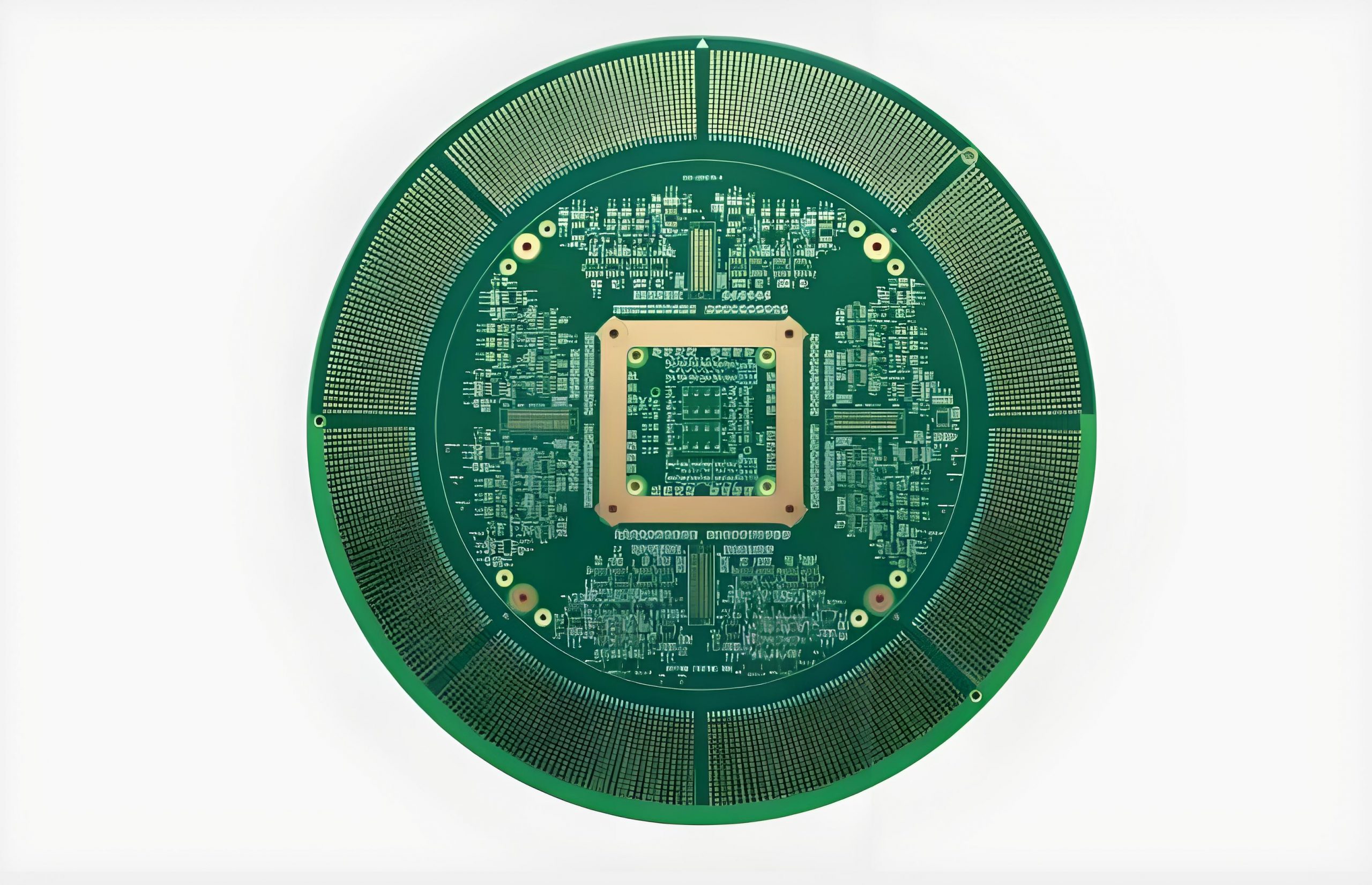
HDI PCB, short for High-Density Interconnect Printed Circuit Board, is a specialized type of circuit board designed to accommodate complex electronic designs with densely packed components and fine-line circuitry. HDI PCB achieves this through advanced manufacturing techniques like microvias, sequential lamination, and laser drilling, enabling higher signal integrity and reduced size compared to traditional PCBs. In AI server motherboards, HDI PCB technology becomes essential for handling high-speed data transmission and thermal management while maintaining compact form factors. The precision and reliability of HDI PCB make it ideal for applications requiring miniaturization without sacrificing performance, particularly in cutting-edge fields like artificial intelligence infrastructure. By integrating finer traces and tighter spacing, HDI PCB boards effectively address the escalating demands of modern AI server designs.

What Are Technical Parameters of HDI PCBs?
Technical parameters of HDI PCBs for AI server motherboards:
- Minimum Aperture and Drilling Technology: HDI PCBs utilize laser-drilled microvias with diameters typically ≤150μm, enabling precise layer interconnections in compact spaces. Traditional PCBs rely on mechanical drilling for ≥200μm holes, limiting routing density.
- Trace Width and Spacing: HDI PCBs achieve ultra-fine line widths and spacings of ≤75μm, allowing for tighter circuit routing and improved signal integrity. Traditional PCBs use ≥100μm traces, which occupy more surface area and restrict component density.
- Pad Density and Component Integration: With pad densities exceeding 20 pads per cm², HDI PCBs accommodate high-pin-count components like BGAs and fine-pitch connectors. Traditional PCBs, with densities below 10 pads per cm², struggle to support modern AI hardware requiring dense I/O interfaces.
- Interlayer Connection Methods: HDI PCBs employ advanced interlayer connections, including blind vias, buried vias, and stacked microvias, to optimize space and reduce signal path lengths. Traditional PCBs primarily use through-hole vias, which consume more board real estate and limit routing flexibility.
- Material and Thermal Performance: HDI PCBs for AI servers incorporate high-Tg laminates and low-loss dielectric materials to withstand thermal stresses from high-power components. Traditional PCBs often use standard FR-4 materials with lower thermal stability, risking deformation under prolonged operation.
- Signal Integrity and High-Speed Design: HDI PCBs are engineered for controlled impedance and low dielectric loss, critical for supporting multi-gigabit data rates in AI servers. Traditional PCBs, with their looser tolerances, may struggle with signal degradation at high frequencies.
How to Achieve 25Gbps Signal Integrity in Your HDI PCB Design?
Below are methods about how to achieve 25 Gbps signal integrity in your HDI PCB design:
- Material Selection for Low-Loss Performance: Prioritize high-frequency laminates with low dielectric constants (DK) and dissipation factors (DF), such as Megtron 6 or Panasonic R5775. These materials minimize signal attenuation and skew at 25Gbps, ensuring cleaner data transmission across long traces. Avoid standard FR-4 for high-speed layers to prevent excessive insertion loss.
- Layer Stack-Up Optimization: Design a symmetric layer stack-up with tightly coupled power and ground planes to reduce electromagnetic interference (EMI). Dedicate specific layers for high-speed differential pairs, isolating them from noisy power domains. Use sequential lamination to embed microvias close to signal layers, shortening return paths and improving impedance control.
- Controlled Impedance Routing: Maintain precise trace widths and dielectric thicknesses to achieve 50Ω or 100Ω differential impedance. For 25Gbps signals, target 6-8mil trace widths with 4-5mil spacing for microstrip or stripline geometries. Leverage impedance calculation tools to validate designs before fabrication, ensuring consistency across the board.
- Via Design for Minimal Stub Effects: Employ blind vias or backdrilled through-hole vias to eliminate via stubs, which cause reflections at high frequencies. Laser-drilled microvias (≤150μm diameter) reduce parasitics and enable denser routing. Avoid excess via counts in high-speed channels to prevent impedance discontinuities.
- Differential Pair Routing: Route 25Gbps differential pairs with matched lengths (≤5mil mismatch) and consistent spacing (≥3x trace width) to minimize skew and crosstalk. Avoid sharp bends (use 45° angles) and maintain isolation from adjacent signals by ≥5x trace width. Implement length tuning with serpentine patterns only when necessary, keeping amplitudes minimal to preserve signal quality.
- Power Integrity and Decoupling: Place low-ESL decoupling capacitors (0402 or 0201 packages) close to high-speed IC power pins. Use stitched ground planes and isolated power islands to reduce noise coupling. For AI server motherboards, distribute power via multiple low-inductance planes to handle transient currents from AI accelerators.
- Thermal Management: Integrate thermal vias beneath high-power components (e.g., SerDes chips) to conduct heat to inner or outer layers. Use heavy copper planes (≥2oz) for power-hungry regions and ensure adequate airflow around the HDI PCB. Excessive heat can degrade signal integrity by altering dielectric properties.
- Pre-Layout Simulation and Post-Layout Verification: Perform SI/PI simulations using tools like Ansys SIwave or Keysight ADS to model channel loss, reflections, and EMI. Validate designs with eye diagram analysis and compliance testing for standards like IEEE 802.3bj or CEI-25G-LR. Iterate on layouts based on simulation results to mitigate risks before prototyping.
- Fabrication Tolerances and Documentation: Specify tight manufacturing tolerances (e.g., ±10% for impedance, ±2mil for trace/space) in your fab notes. Collaborate with PCB vendors experienced in HDI processes to ensure laser drilling accuracy and lamination consistency. Provide clear documentation on stack-up, via types, and controlled impedance requirements to avoid misinterpretation.
How to Optimize HDI Blind and Buried Design For High Precision Interconnects?
Here are methods about how to optimize HDI blind and buried design for high precision interconnects:
- Prioritize Layer Stack-Up Symmetry: Design your HDI PCB with balanced layer counts above and below the core to minimize warpage and improve signal integrity. Symmetric stack-ups reduce residual stress during lamination, ensuring consistent via registration and reliability for blind and buried vias.
- Optimize Blind Via Placement: Position blind vias near high-speed components to shorten signal paths and reduce parasitic capacitance. Avoid clustering blind vias in dense regions to prevent etching or drilling inaccuracies. Use staggered arrangements to maintain adequate spacing between adjacent vias.
- Leverage Buried Vias for Density: Integrate buried vias to connect inner layers without occupying surface space, freeing up routing channels for critical signals. This approach is particularly effective for AI server motherboards requiring dense power distribution networks and high-speed interconnects.
- Control Aspect Ratios: Limit blind via aspect ratios (depth-to-diameter) to ≤1:1 to ensure reliable plating and avoid voids. For buried vias, maintain aspect ratios ≤0.8:1 to prevent misregistration during sequential lamination cycles.
- Use Laser Drilling for Precision: Employ UV or CO2 laser drilling for blind vias to achieve diameters as small as 50μm. This enhances routing flexibility in high-density BGA and fine-pitch connector areas. Verify laser drilling accuracy with microsection analysis before mass production.
- Implement Backdrilling for Stub Reduction: Apply controlled-depth backdrilling to remove via stubs from through-hole vias used in high-speed channels. This technique reduces signal reflections and improves impedance continuity at 25Gbps and beyond.
- Isolate Power and Ground Planes: Dedicate specific layers to power and ground planes near blind via regions to minimize noise coupling. Use stitched connections between planes to create low-impedance return paths for high-frequency signals.
- Validate with Thermal Simulation: Simulate heat dissipation around blind and buried via areas using thermal analysis tools. Ensure copper fill and thermal vias are strategically placed to prevent hotspots near high-power components like AI accelerators.
- Collaborate with Fabricators Early: Engage HDI PCB manufacturers during the design phase to align on capabilities such as laser drilling accuracy, lamination cycles, and plating uniformity. Provide detailed documentation on via types, stack-up requirements, and impedance targets.
- Test for Signal Integrity: Perform time-domain reflectometry (TDR) and eye diagram testing on prototype boards to validate via performance. Focus on blind via transitions and buried via interconnections to identify potential impedance discontinuities.
Why Choose HDI PCB Board for AI Server Motherboard?
Reasons for why choose HDI PCB board for AI server motherboard:
- Maximize Component Density: HDI PCBs enable tighter placement of high-pin-count components like BGAs and AI accelerators, freeing space for additional memory modules or cooling solutions. This density reduces the board footprint while supporting cutting-edge silicon.
- Ensure Signal Integrity at High Speeds: With controlled impedance traces and low-loss materials, HDI PCBs minimize signal degradation in 25Gbps+ channels. This prevents data errors in AI workloads, where split-second precision drives real-time inference and training.
- Reduce Power Consumption: Shorter signal paths and optimized via structures lower switching losses in high-frequency circuits. For AI servers operating 24/7, this efficiency translates to measurable savings in energy costs and thermal management expenses.
- Improve Thermal Performance: HDI PCBs integrate thermal vias and heavy copper layers to dissipate heat from power-hungry AI chips. This prevents thermal throttling, ensuring consistent performance during peak computation periods like model training or large-scale simulations.
- Enhance Reliability in Harsh Environments: Advanced HDI manufacturing processes, including laser drilling and sequential lamination, improve via reliability and reduce solder joint fatigue. For data centers with strict uptime requirements, this means fewer maintenance cycles and longer service life.
- Support Future-Proof Scalability: HDI PCBs accommodate emerging interface standards like PCIe 5.0 and CXL without redesigns. Their modular layer stack-ups allow easy integration of next-gen AI accelerators, protecting your investment as technology evolves.
- Streamline Supply Chain Efficiency: Partnering with HDI PCB specialists ensures access to advanced capabilities like microvia filling and embedded capacitance. This reduces reliance on multiple vendors, simplifying procurement and accelerating time-to-market for AI server products.
How to Improve HDI PCB Reliability for AI servers under Heavy Loads?
Here are tips about how to improve HDI PCB reliability for AI servers under heavy loads:
- Select High-Performance Materials: Use laminates with high glass transition temperatures (TG ≥ 170°C) and low dielectric loss to resist thermal degradation during prolonged AI workloads. Incorporate ceramic-filled prepregs to enhance thermal conductivity and reduce z-axis expansion.
- Optimize Layer Stack-Up for Thermal Management: Design symmetric layer stacks with embedded ground/power planes near high-speed layers to dissipate heat efficiently. Dedicate inner layers to heavy copper fills (≥2oz) for power distribution, minimizing voltage drop and heat buildup.
- Implement Robust Via Structures: Strengthen via reliability with laser-drilled microvias filled with conductive paste or copper plating. Use staggered blind via arrays to reduce stress concentrations and prevent barrel cracking under thermal cycling.
- Enhance Solder Joint Fatigue Resistance: Apply ENEPIG (Electroless Nickel Electroless Palladium Immersion Gold) surface finish to improve solderability and resist corrosion in high-temperature environments. Optimize BGA pad designs with non-solder mask defined (NSMD) geometries for better stress relief.
- Control Impedance and Crosstalk: Maintain tight impedance tolerance (±5%) across differential pairs using coupled stripline geometries. Isolate high-speed channels from noisy domains with guard traces and stitched ground planes, reducing crosstalk in dense AI accelerator regions.
- Incorporate Thermal Vias and Heat Slugs: Place arrays of thermal vias (≥0.2mm diameter) under power-hungry components like GPUs or HBM modules. Integrate copper heat slugs directly into the PCB stack-up to conduct heat to external heat sinks or liquid cooling systems.
- Validate with Accelerated Stress Testing: Subject prototypes to thermal cycling (-55°C to +125°C, 1,000 cycles) and power temperature cycling (PTC) to simulate years of AI server operation. Use scanning acoustic microscopy (SAM) to detect delamination in hidden via structures.
- Leverage Advanced Manufacturing Techniques: Partner with fabricators using plasma etching for via desmear, ensuring clean sidewalls for reliable plating. Require automated optical inspection (AOI) and X-ray systems to validate microvia integrity and layer registration.
- Design for Manufacturability (DFM): Provide clear DFM guidelines to fabricators, including minimum annular ring (≥50μm for blind vias) and solder mask dam specifications (≥75μm). Avoid hairline traces (≤50μm) in high-stress areas to prevent etching undercut.
- Monitor In-Field Performance: Implement built-in temperature sensors and current monitors on the PCB to track hotspots during AI training sessions. Use edge computing platforms to analyze real-time thermal data and trigger predictive maintenance alerts.
How to Improve Manufacturing Yield and Reduce Costs for AI Server Motherboard?
Below are methods about how to improve manufacturing yield and reduce costs for AI server motherboard:
- Simplify Layer Stack-Up Design: Reduce unnecessary layers by consolidating power/ground planes and using buried vias to route inner signals. Fewer layers lower lamination cycles and material costs while simplifying impedance control for consistent yields.
- Standardize Component Placement: Reuse proven BGA footprints and connector positions across AI server motherboard revisions. Standardization minimizes custom stencil and fixture costs while accelerating assembly line setup.
- Optimize Panel Utilization: Maximize PCB panel space by arranging multiple motherboard designs with common outlines. Use edge-to-edge routing and shared coupons to reduce wasted material during etching and drilling.
- Implement Design for Manufacturing (DFM) Rules: Enforce minimum trace/space (≥50μm) and annular ring (≥60μm) rules compatible with standard HDI processes. Avoid hairline features that require costly specialty equipment or yield-sapping etch compensation.
- Adopt Plated-Through-Hole (PTH) Alternatives: Replace through-hole connectors with press-fit pins or surface-mount alternatives to eliminate costly PTH drilling and plating steps. This reduces cycle time and improves hole wall quality.
- Leverage Automated Optical Inspection (AOI): Deploy AOI systems post-etch and post-soldermask to detect defects like under-etching or mask misalignment. Early detection prevents costly rework at later stages like assembly.
- Negotiate Volume Contracts with Suppliers: Secure discounts on laminates, copper foil, and dry film by committing to annual usage volumes. Bundle orders for AI server motherboards with other products to leverage economies of scale.
- Outsource Non-Core Processes: Partner with specialists for laser drilling, sequential lamination, and heavy copper plating instead of investing in in-house capacity. Focus internal resources on high-value design and testing.
- Reduce Prototype Iterations: Use virtual prototyping tools to simulate via reliability, thermal performance, and signal integrity before fabrication. Fewer physical prototypes lower engineering costs and speed time-to-market.
- Implement Lean Inventory Practices: Adopt just-in-time (JIT) delivery for raw materials and finished PCBs to minimize warehousing costs. Use kanban systems to align production with AI server assembly schedules.
- Train Engineering Teams on Yield Fundamentals: Invest in training programs to teach designers about HDI process limitations, such as aspect ratio constraints or microvia plating challenges. Better-informed designs reduce scrap rates.
- Recycle Scrap Material: Partner with recyclers to reclaim copper from etched-off panels and rejected boards. Revenue from recycled materials offsets raw material costs over time.
How to Solve Micro-Via and Fine-Line Production Challenges in HDI PCBs for AI servers?
- Use Advanced Laser Drilling Systems: Invest in UV or CO2 laser drilling machines with high pulse frequency and beam steering capabilities. These systems achieve ≤25μm microvia diameters with minimal taper, ensuring precision for fine-pitch AI components.
- Optimize Electroless Copper Plating: Implement direct metallization processes to eliminate traditional drill debris and improve via wall adhesion. This reduces voids in blind microvias, a common failure point in high-density AI server boards.
- Control Etching Uniformity: Use alternating spray etchers with precise nozzle spacing and chemical concentration monitoring. This maintains consistent trace profiles (≥40μm lines/spaces) across large AI motherboard panels, preventing over-etching in fine-line regions.
- Adopt Semi-Additive Process (SAP) for Fine Lines: Replace subtractive etching with SAP to build 35μm traces using pattern plating and flash etching. This method reduces sidewall undercut and improves yield in dense BGA breakout areas.
- Improve Laminate Registration: Select laminates with low coefficient of thermal expansion (CTE ≤12ppm/°C) to minimize layer misalignment during sequential lamination. This ensures microvia-to-trace alignment within 25μm tolerance for AI accelerator interfaces.
- Implement Automated Optical Shaping (AOS): Deploy AOS systems post-etch to repair neckdowns and open circuits in fine-line areas. This reduces scrap rates by addressing defects before layer stacking in complex HDI builds.
- Partner with Process-Specialized Fabricators: Select PCB manufacturers with expertise in via-in-pad plating and laser ablation for buried microvias. Their experience reduces trial-and-error cycles, accelerating time-to-market for AI server motherboards.
Conclusion
In summary, HDI PCB technology is revolutionizing AI server motherboards with its high-density interconnects, superior signal integrity, and enhanced thermal management capabilities. From advanced micro-via designs to optimized blind/buried vias, these boards deliver the performance and reliability required for heavy AI workloads. For manufacturers seeking cutting-edge HDI solutions with cost-efficient production, EBest Circuit (Best Technology) offers industry-leading expertise in ultra-fine 25/25μm trace designs and high-yield fabrication. Contact our team today for customized HDI PCB solutions that power your AI infrastructure with uncompromising quality and accelerated delivery: sales@bestpcbs.com.
Tags: HDI PCB, HDI PCB Board