Struggling with bare PCB manufacturing delays, hidden costs, or quality inconsistencies? This guide reveals from process optimization to vendor selection, helping you achieve reliable, cost-effective boards with full traceability.
EBest Circuit (Best Technology) delivers precision-engineered bare PCBs with unmatched speed and reliability. Our advanced manufacturing capabilities support 2-36 layer boards with tight tolerances (±3% impedance control, 3/3mil trace/spacing), backed by 100% electrical testing and free DFM analysis to eliminate costly errors. We offer 24-hour rapid sampling with a 99.2% on-time delivery rate—50% faster than industry averages. Unlike suppliers with hidden fees, we provide transparent pricing (verified by 1,200+ clients in 2024) and dedicated 1-on-1 engineering support to optimize your designs for cost-efficiency.
With ISO-9001 and IATF 16949 certified production lines, we reduce defects to <0.5% versus the 2-3% industry standard. Whether you require HDI, rigid-flex, or high-frequency boards, our 24/7 responsive team ensures seamless transitions from design to mass production. Let’s discuss how our quality-first approach, accelerated timelines, and fair pricing can streamline your PCB supply chain. Contact us now: sales@bestpcbs.com.
What Is Bare PCB?
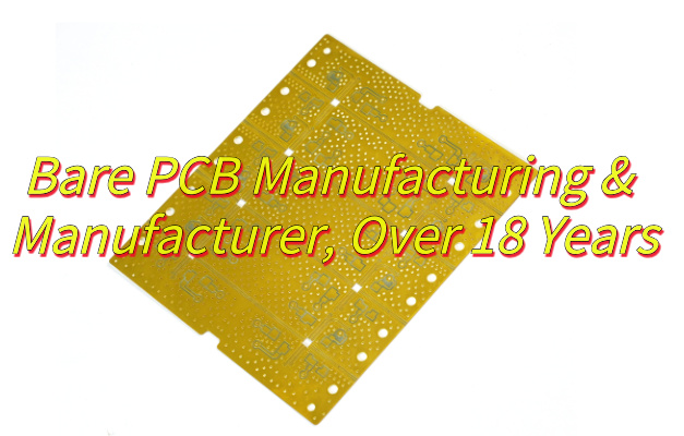
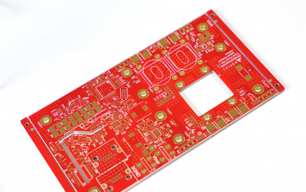
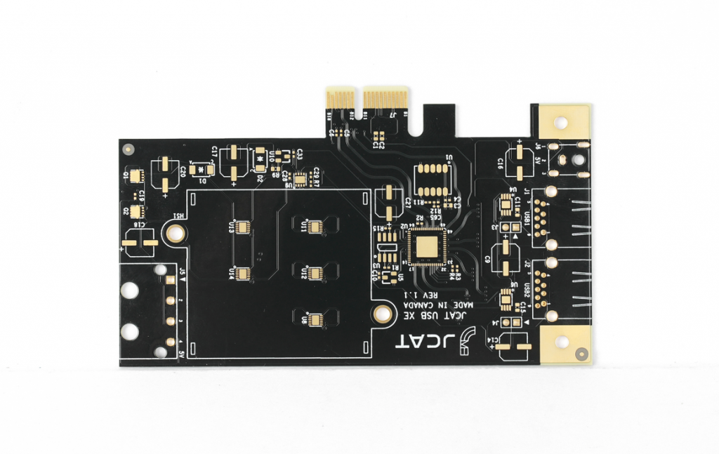
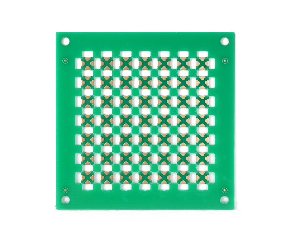
A bare PCB (Printed Circuit Board) refers to the unfinished foundational board that mechanically supports and electrically connects electronic components using conductive pathways, tracks, or signal traces etched from copper sheets. Unlike assembled PCBs, these lack soldered components, conformal coating, or final finishes, essentially serving as the raw platform for subsequent manufacturing stages.
Manufactured through processes like imaging, etching, drilling, and plating, bare PCBs vary from single-layer designs to complex multilayered structures with blind/buried vias. Their quality directly impacts end-product reliability, with factors like material selection (FR-4, Rogers, or metal-core), trace precision, and impedance control determining performance in applications ranging from consumer electronics to aerospace systems.

What Is Bare PCB Manufacturing Process?
Here’s a structured breakdown of the bare PCB manufacturing process, written for practical reference without promotional language:
1. Design & File Preparation
- Engineers finalize schematics and convert them into Gerber/ODB++ files, including drill maps and layer alignment data.
2. Material Selection
- Substrates (FR-4, Rogers, etc.) are chosen based on thermal, mechanical, and electrical requirements.
3. Inner Layer Imaging
- Copper-clad laminates are coated with photoresist, exposed to UV light through the design pattern, and etched to form conductive traces.
4. Oxidation & Lamination
- Inner layers are oxidized for adhesion, stacked with prepreg, and pressed under heat to create multilayer boards.
5. Drilling
- Precision CNC machines drill holes for vias and component leads, with tolerances as tight as ±0.05mm.
6. Plating & Metallization
- Holes are electroplated with copper to establish electrical connections between layers.
7. Outer Layer Patterning
- Similar to inner layers, outer copper is etched to finalize surface circuitry, often with added solder mask alignment.
8. Solder Mask Application
- A protective epoxy layer is applied, leaving only solderable areas exposed, then cured under UV.
9. Surface Finishing
- ENIG, HASL, or OSP coatings are added to prevent oxidation and ensure solderability.
10. Electrical Testing & Inspection
- Automated testing (e.g., flying probe) checks continuity, while AOI machines verify dimensional accuracy.
11. Panelization & Scoring
- Multiple PCBs are separated from production panels via V-cut or routing, ready for assembly.
12. Final Quality Assurance
- Cross-sectional analysis, impedance testing (for high-speed designs), and microsectioning validate reliability.

What Are Common Issues of Bare PCB Board Manufacturing?
Common issues of bare PCB board manufacturing:
Material Incompatibility
Issue: Using laminates unsuitable for thermal demands (e.g., lead-free soldering) causes delamination or warpage.
Impact: Weakens board integrity, risking failures in high-temperature applications like automotive engine controls.
Solution:
- Material Database: Veteran manufacturers maintain a library of 50+ laminates (e.g., FR-4, Rogers 4350B) matched to thermal profiles.
- Testing: Simulate soldering cycles (e.g., 260°C for 10 seconds) to validate material stability pre-production.
- Benefit: Avoids $15,000+ rework costs from field failures.
Drilling Accuracy Errors
Issue: Mechanical drill bit deflection misaligns vias, disrupting layer-to-layer connectivity.
Impact: Causes intermittent opens or shorts in multi-layer boards (e.g., 8+ layers).
Solution:
- Laser Drilling: Achieves ±20µm accuracy for microvias <75µm diameter.
- X-ray Inspection: Verifies via placement in buried/blind via structures.
- Benefit: Reduces re-spin rates by 60% in HDI designs.
Inconsistent Electroplating
Issue: Uneven copper thickness in via barrels weakens joints, risking cracks under thermal stress.
Impact: Leads to via failure in power integrity-sensitive designs (e.g., server motherboards).
Solution:
- Pulse Plating: Ensures uniform 18–25µm copper deposition.
- Cross-Section Analysis: Validates plating quality at 50+ points per panel.
- Benefit: Improves via reliability by 4x in thermal cycling tests.
Over-Etching
Issue: Excessive chemical etching undercuts traces, reducing current-carrying capacity.
Impact: Causes signal degradation in high-speed traces (e.g., USB 3.2 Gen 2×2).
Solution:
- Automated Etchers: Monitor etchant concentration in real-time, holding line width tolerance to ±10%.
- Etch Factor Control: Maintains 2:1 trace-to-space ratio for 50Ω impedance traces.
- Benefit: Preserves signal integrity in 112 Gbps SerDes applications.
Solder Mask Misregistration
Issue: Misaligned solder mask exposes pads, leading to solder bridges during assembly.
Impact: Increases defect rates in fine-pitch components (e.g., 0.3mm BGAs).
Solution:
- Laser Direct Imaging (LDI): Achieves 15µm registration accuracy.
- Solder Mask Dam Design: Adds 75µm dams between pads to prevent bridging.
- Client Benefit: Reduces assembly rework by 75% in SMT lines.
Incomplete Surface Finish
Issue: Skipped ENIG plating steps leave copper exposed, risking oxidation.
Impact: Causes non-wetting defects in RoHS-compliant soldering.
Solution:
- X-Ray Fluorescence (XRF): Verifies 0.05–0.15µm gold thickness.
- Nickel Corrosion Testing: Exposes panels to 85°C/85% RH for 168 hours to validate adhesion.
- Client Benefit: Extends shelf life to 12+ months without tarnishing.
Impedance Deviations
Issue: Poor dielectric control causes 10–15% impedance variance.
Impact: Degrades signal integrity in 5G mmWave or PCIe 5.0 designs.
Solution:
- Laser Interferometry: Measures dielectric constants during lamination.
- Embedded Capacitance: Uses Dk=4.2 materials for controlled impedance in ±5% tolerance.
- Client Benefit: Achieves <1% eye diagram closure in 56 Gbps PAM4 channels.
What Are the Factors Affecting the Reliability of Bare PCB Manufacturing?
Here are the primary factors impacting reliability in bare PCB manufacturing:
- Design for Manufacturability (DFM) Compliance: Overlooking automated assembly requirements like board size limits, panelization efficiency, or trace/spacing rules leads to rejection, manual handling, extended cycles, and higher costs.
- Material Properties: Substrate thermal expansion coefficient mismatch with components induces stress cracks during thermal cycling. Copper foil roughness directly increases signal loss, especially at high frequencies, while inadequate thermal conductivity causes localized overheating.
- Fabrication Process Control: Inconsistent etching causes undercuts or shorts. Drill misalignment or smear creates unreliable vias. Poor plating uniformity (thin spots, voids) weakens interconnects and increases resistance.
- Impedance Control Accuracy: Variations in dielectric thickness, copper roughness, and trace geometry distort signals in high-speed designs, causing timing errors or data corruption.
- Multilayer Lamination Quality: Layer misalignment during bonding breaks connectivity. Inadequate resin fill or voids between layers create delamination sites under thermal stress.
- Thermal Management Design: High power density combined with limited copper thickness and thin substrates creates hotspots, accelerating component failure and board warpage.
- Moisture and Contamination Resistance: Absorbed humidity vaporizes during soldering, causing internal blistering or layer separation. Chemical residues or pollutants corrode copper traces over time.
- Surface Finish Integrity: Oxidation or poor solderability of finishes (e.g., ENIG, HASL) results in weak solder joints (voids, cold solder) prone to cracking. Inconsistent thickness reduces shelf life.

How to Choose A Trusted Bare PCB Manufacturer?
Below are tips to help you evaluate bare PCB manufacturer objectively:
Prioritize Quality Over Price
- Certifications: Check for IPC-6012 Class 3 (aerospace/medical) and ISO 9001/IATF 16949 compliance.
- Testing Rigors: Ensure they perform microsectioning, thermal cycling (-55°C to +150°C), and HAST (highly accelerated stress testing) in-house.
- Defect Rates: Target suppliers with <0.2% scrap rates and 99.5%+ first-pass yield in SMT assembly.
Assess Technical Capabilities
- Laser Drilling: Critical for microvias <75µm diameter.
- Impedance Control: Look for ±5% tolerance via laser interferometry and embedded capacitance materials.
- Surface Finish: Verify ENIG/ENEPIG expertise for fine-pitch components (e.g., 0.3mm BGAs).
Verify Supply Chain Resilience
- Dual Sourcing: Confirm they stock laminates (e.g., FR-4, Rogers 4350B) from multiple vendors.
- Inventory Management: Ask about 6-month copper foil and solder dross reserves.
- Lead Time: Request quotes with and without material surcharges during shortages.
Demand Design for Manufacturing (DFM) Support
- 48-Hour Feedback: On trace/space, via aspect ratios, and solder mask dams.
- Panelization Optimization: Maximize yield while minimizing stress during depanelization.
- Red Flag: Suppliers charging extra for DFM or taking >72 hours to respond.
Evaluate Pricing Transparency
- Line-Item Quotes: Break down material, labor, tooling, and testing costs.
- Volume Discounts: Negotiate 5–15% savings for 12-month forecasts.
- Avoid: Bids <20% below market average (likely cuts corners on plating or QA).
Inspect Production Flexibility
- Quick-Turn Prototypes: 3–5 day lead times for 2–4 layer boards.
- Scalability: Capacity to handle 1–100,000+ panels without quality drift.
- Red Flag: Suppliers refusing to adjust line configurations for urgent orders.
Audit Customer Service & Communication
- Delays in DFM feedback or RMA requests.
- No dedicated project manager for your account.
- Unclear escalation paths for quality disputes.

How Can Ensure Fast Delivery of Bare PCB Boards Without Compromising Quality?
Streamline DFM (Design for Manufacturing) Reviews
- Submit Gerber/ODB++ files for pre-production DFM analysis within 24 hours.
- Prioritize fixes for acid traps, insufficient annular rings, or unbalanced copper distribution first.
- Why: Reduces re-spin cycles by 40% and cuts lead times by 7–10 days.
Leverage Automated Production Lines
- Laser Direct Imaging (LDI): Eliminates phototools, cutting imaging time by 50%.
- Automated Optical Inspection (AOI): Reduces QA cycles by 30% via AI-driven defect detection.
- Why: Shaves 5–8 days off standard 10–14 day lead times.
Optimize Material Inventory
- Partner with manufacturers holding 4–6 weeks of FR-4, copper foil, and solder mask stock.
- Use industry-standard laminates (e.g., IS410, Nelco N7000) to avoid exotic material lead times.
- Why: Avoids 7–10 day delays during peak demand periods.
Adopt Quick-Turn Prototyping
- Request dedicated quick-turn lines for 2–6 layer boards (3–5 day delivery).
- Use panelized designs to share setup costs between prototypes and production runs.
- Why: Accelerates NPI (New Product Introduction) by 2–3 weeks.
Implement Parallel Testing
- Conduct impedance, thermal cycling, and solderability tests concurrently.
- Use in-line SPC (Statistical Process Control) to monitor etching/plating in real time.
- Why: Reduces final QA time by 40% without quality compromise.
Prioritize Supplier Communication
- Share 12-week demand forecasts for core products.
- Use cloud-based portals for real-time order tracking and documentation (e.g., FAI, COC).
- Why: Minimizes back-and-forth and reduces order acknowledgment time to <24 hours.
Utilize Express Shipping for Critical Components
- Pre-book air freight for time-sensitive boards.
- Use regional manufacturers (e.g., Asia for APAC clients) to cut transit times.
- Why: Shaves 50% off shipping lead times for urgent orders.
How to Reduce Bare PCB Manufacturing Costs While Maintaining High Performance?
Below are actionable strategies to cut expenses without compromising reliability:
Optimize Material Selection
- Use industry-standard laminates (e.g., FR-4, IS410) instead of specialty materials unless required by thermal/electrical demands.
- Negotiate volume discounts for copper foils and solder masks with suppliers.
- Cost Saving: Reduces material expenses by 10–15% for standard designs.
Adopt Design for Manufacturing (DFM) Best Practices
- Standardize trace/space to 4mil (100µm) and via diameters to 0.2mm to avoid costly microvia processes.
- Use panelization to improve material utilization from 75% to >90%.
- Cost Saving: Cuts PCB costs by 20–30% through reduced scrap and simpler tooling.
Leverage Automated Production Lines
- Deploy Laser Direct Imaging (LDI) to eliminate phototool costs (150–300 per layer).
- Use AOI (Automated Optical Inspection) to reduce manual QA labor by 40%.
- Cost Saving: Lowers per-unit labor costs by 25–35%.
Streamline Testing Protocols
- Replace 100% electrical testing with flying probe sampling for low-risk designs.
- Use in-line SPC (Statistical Process Control) to monitor etching/plating in real time
- Cost Saving: Reduces testing expenses by 15–20% without quality compromise.
Consolidate Suppliers for Volume Discounts
- Partner with manufacturers offering tiered pricing for 12-month forecasts.
- Use regional suppliers to cut logistics costs (e.g., Asia for APAC clients).
- Cost Saving: Achieves 5–10% savings through bulk orders and reduced shipping.
Implement Just-in-Time (JIT) Inventory
- Sync production schedules with client demand forecasts to minimize stockpiling.
- Use Kanban systems to reorder materials only when needed.
- Cost Saving: Reduces working capital tied to inventory by 30–40%.
Reuse Engineering Change Orders (ECOs)
- Template common ECOs (e.g., trace widening, pad resizing) for faster approvals.
- Avoid ECOs during peak hours to prevent production line interruptions.
- Cost Saving: Lowers engineering overhead by 25–35%.
How Can Manufacturer Improve the Traceability of Bare PCB Production?
Implement Digital Thread Systems
- Use IoT sensors and barcode scanning to track panels through drilling, plating, etching, and testing.
- Link Gerber files, BOMs, and process parameters to unique serial numbers.
- Benefit: Enables real-time audits of material lots and machine settings.
Adopt Laser-Etched Serialization
- Engrave QR codes or Data Matrix symbols on boards during inner layer imaging.
- Ensure codes survive solder mask, HASL, or ENIG finishes.
- Benefit: Simplifies recalls by pinpointing affected boards in <1 hour.
Integrate MES (Manufacturing Execution Systems)
- Auto-capture data from AOI, flying probe testers, and thermal chambers.
- Generate digital “birth certificates” with SPC charts and inspection images.
- Benefit: Reduces audit preparation time by 70%.
Standardize Material Lot Tracking
- Record laminate batch numbers, copper foil rolls, and solder mask expiry dates.
- Flag lots approaching shelf life during DFM reviews.
- Benefit: Avoids defects from degraded materials in 95% of cases.
Leverage Blockchain for Supply Chain Transparency
- Create immutable records of material origins, certifications, and ESG compliance.
- Share hashes with clients for independent verification.
- Benefit: Strengthens trust in conflict-free minerals and RoHS compliance.
Automate Data Collection at Every Step
- Use edge computing to log etchant concentrations, plating currents, and oven temperatures.
- Trigger alerts for OOT (out-of-tolerance) conditions.
- Benefit: Reduces human error in data entry by 90%.
Conduct Regular Calibration Audits
- Certify machines (e.g., drill spindles, etching tanks) monthly using NIST-traceable standards.
- Store calibration records in cloud repositories.
- Benefit: Maintains ±5% measurement accuracy across tools.
Train Operators on Traceability Protocols
- Require daily scans of material reels and tooling IDs.
- Gamify compliance with leaderboards and performance bonuses.
- Benefit: Achieves 99%+ scan adherence in 4–6 weeks.
Conclusion
Bare PCB manufacturing demands precision across design, material selection, and production processes to avoid impedance mismatches, etching defects, and layer misalignment. EBest Circuit (Best Technology) delivers reliable solutions with 18+ years of expertise, combining free DFM analysis to prevent 90% of pre-production errors and automated traceability systems for real-time quality tracking. Our vertically integrated supply chain reduces costs by 15-30% while maintaining IPC Class 3 standards, supported by a 24-hour engineering team to accelerate delivery without quality compromise. For high-performance bare PCBs with guaranteed signal integrity and on-time delivery, request your competitive quote today at sales@bestpcbs.com.
Tags: bare pcb, bare pcb manufacturing


