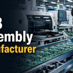
PCB or Printed Circuit Board assembly at EBest Circuit (Best Technology) involves combining the bare PCB, electronic components, and other accessories effectively to allow the assembly to function as the designer intended. Generally speaking, the fabrication methods involve a number of major steps:
(1)Component placement
(2)Soldering
(3)Cleaning
(4)Inspection
(5)Testing
Component Placement
Methods of placing components on the PCB rely on several factors such as:
Single or double side component placement
SMD components only
Through-hole (TH) components only
Mix of SMD and through-hole components
A PCB may have components present only on one of its sides or on both, although assembling a PCB with through-hole components on both sides is a rare occurrence. Single side component placement with either all SMDs or all through-hole components is more common, while single sided PCBs with a mix of SMDs and through-hole components is also to be found.
For assemblies requiring SMDs on both sides of the PCB or a mix of SMD and through-hole components on the top and only SMDs on the bottom, the PCB assembly process must be broken up into several intermediate steps, and the assembler needs to take special precautions for each of them.
Soldering
Soldering is the process of joining two dissimilar metals using a molten filler metal alloy. The molten metal alloy enters the joint, and as it cools and solidifies, bonds with the adjoining metals. Primarily,  three common ways of soldering including manual soldering, wave soldering and reflow soldering are available.
Cleaning
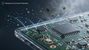
After soldering is over, some flux residue may remain on the printed circuit board. Over time, this can turn acidic, and corrosively damage solder joints. The flux residue can also attract fingerprints and make the PCB look unclean.
Manual Inspection
Inspection is necessary at various stages of assembly. For instance, one stage of inspection is necessary when the operator has stuffed TH components into the board, and again once the assembly has undergone wave soldering.
Similarly, for reflow soldering, inspection is necessary once after solder paste printing is over, then again after mounting the SMD components, and once again after the boards have exited the reflow oven.
AOI & X-Ray Inspection
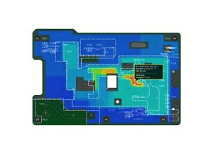
For large batches of PCB assembly, the manual inspection process may be too slow. A faster process is the Automatic Optical Inspection or AOI process. AOI machines have video cameras to capture images of the PCB, the components, and the solder quality, and they can compare the images with standard images in the machine’s memory. The AOI machines work at high speed processing a large number of PCBs within a relatively short time.
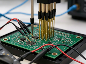
Electrical & Functional Testing
Electrical testing may be necessary after the assembly has passed through the above stages, to test whether the assembly functions as intended by the designer. This may involve programming the board, or calibrating certain components before the actual testing can begin.
Electrical and functional testing involves applying specific voltage/voltages to the circuit on the PCB and looking for normal/abnormal behavior at predefined outputs. Some tests may require a voltmeter and ammeter, while others may need more sophisticated instruments such as an oscilloscope or a waveform analyzer to complete the testing.
Conclusion
PCB assembly is a complicated process involving several technical processes with important setup parameters. Eminent assemblers such as EBest Circuit (Best Technology)Â are always careful with these setup parameters to allow the final product achieve the desired quality.
You may also like

Tags: PCB Assembly, PCB Assembly FAB