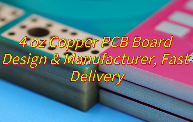
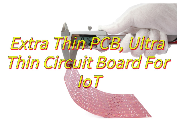
Looking for extra thin PCB solutions? This guide explores ultra-thin circuit board specifications, IoT applications, thermal management, and 5G performance enhancements in compact designs.
At EBest Circuit (Best Technology), we understand your need for reliable yet cost-effective ultra thin circuit boards that power your IoT innovations. Our advanced manufacturing capabilities allow us to produce PCBs as thin as 0.2mm with exceptional precision, ensuring perfect fit for your compact devices while maintaining superior signal integrity. What truly sets us apart is our rigorous quality control process that delivers industry-leading <0.01% defect rates, giving you peace of mind for mass production. We’ve optimized our supply chain to offer these premium ultra-thin boards at prices 15-20% below market average without compromising quality – savings you can pass to your customers or reinvest in R&D. With over 200 successful IoT projects delivered globally, our engineering team can help you solve your most challenging design constraints while meeting tight deadlines. Let’s discuss how our high-performance, competitively priced ultra thin PCBs can give your IoT products an edge in today’s crowded market. Welcome to contact us: sales@bestpcbs.com.
What Is Extra Thin PCB?
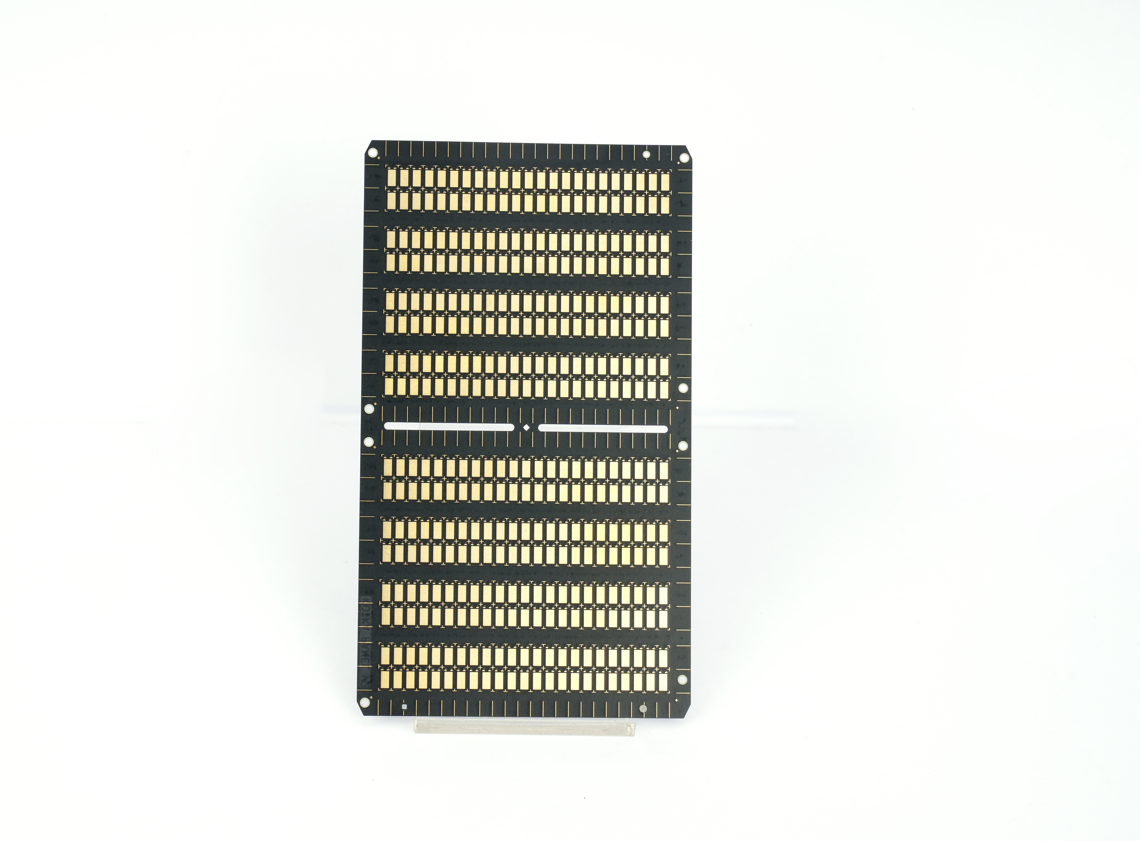
An extra thin PCB is a specialized printed circuit board characterized by an exceptionally slim profile, typically measuring under 0.4 millimeters in total thickness, achieved through precision manufacturing techniques like advanced etching and laser drilling on ultra-thin core materials such as polyimide or specialized laminates. This type of extra thin PCB is engineered specifically for Internet of Things (IoT) applications where extreme miniaturization is essential, enabling direct integration into wearables, implantable medical sensors, and compact environmental trackers where traditional circuit boards would be physically impossible. Designing a robust extra thin PCB requires meticulous attention to thermal dissipation pathways, impedance control, and material selection to ensure reliable operation despite the minimal material volume while maintaining the flexibility and durability needed for dynamic IoT environments, leveraging specialized fabrication processes that preserve electrical integrity even at these extreme thicknesses to support complex circuitry in microscopic footprints.
What Are Specifications of Extra Thin PCB?
Here are the detailed specifications for extra thin PCB:
- Thickness Parameters: An Extra Thin PCB typically measures between 0.1mm to 0.4mm in total thickness, achieved through ultra-precise material layering and etching processes to meet the demands of space-constrained IoT devices.
- Material Composition: These boards often use high-performance polyimide substrates or specialized laminates, providing flexibility and thermal stability while maintaining the structural integrity required for wearable and embedded IoT applications.
- Conductivity & Layer Count: Despite their slim profile, Extra Thin PCBs support multi-layer designs (2-6 layers) with fine-line copper traces (as narrow as 25µm) to ensure reliable signal transmission in compact IoT electronics.
- Thermal Management: Effective heat dissipation is maintained through advanced dielectric materials and optimized copper distribution, preventing overheating in high-density IoT circuits.
- Flexibility & Durability: Designed for dynamic IoT environments, Extra Thin PCBs exhibit excellent bend radius tolerance (down to 1mm) without compromising electrical performance.
- Surface Finishes: Common finishes like ENIG (Electroless Nickel Immersion Gold) or OSP (Organic Solderability Preservative) are applied to enhance solderability and corrosion resistance in humid or variable IoT operating conditions.
- Manufacturing Tolerances: Tight tolerances (±0.05mm for hole positioning, ±10% impedance control) ensure precision alignment with micro-components in IoT sensors and wearables.
- Testing Standards: Each Extra Thin PCB undergoes rigorous electrical testing (continuity, insulation resistance) and mechanical stress tests (flex cycles, thermal shock) to validate IoT-ready reliability.
What Makes Extra Thin PCB Ideal for IoT Devices?
Here’s why extra thin PCBs are perfectly suited for IoT devices, explained from a practical user perspective:
- Space Efficiency: The ultra-slim profile (as thin as 0.1mm) allows seamless integration into compact IoT devices like wearables or smart sensors, freeing up room for batteries and other components without sacrificing functionality.
- Lightweight Design: Their minimal weight reduces strain on portable IoT gadgets, enhancing comfort for wearables and improving energy efficiency for battery-dependent applications.
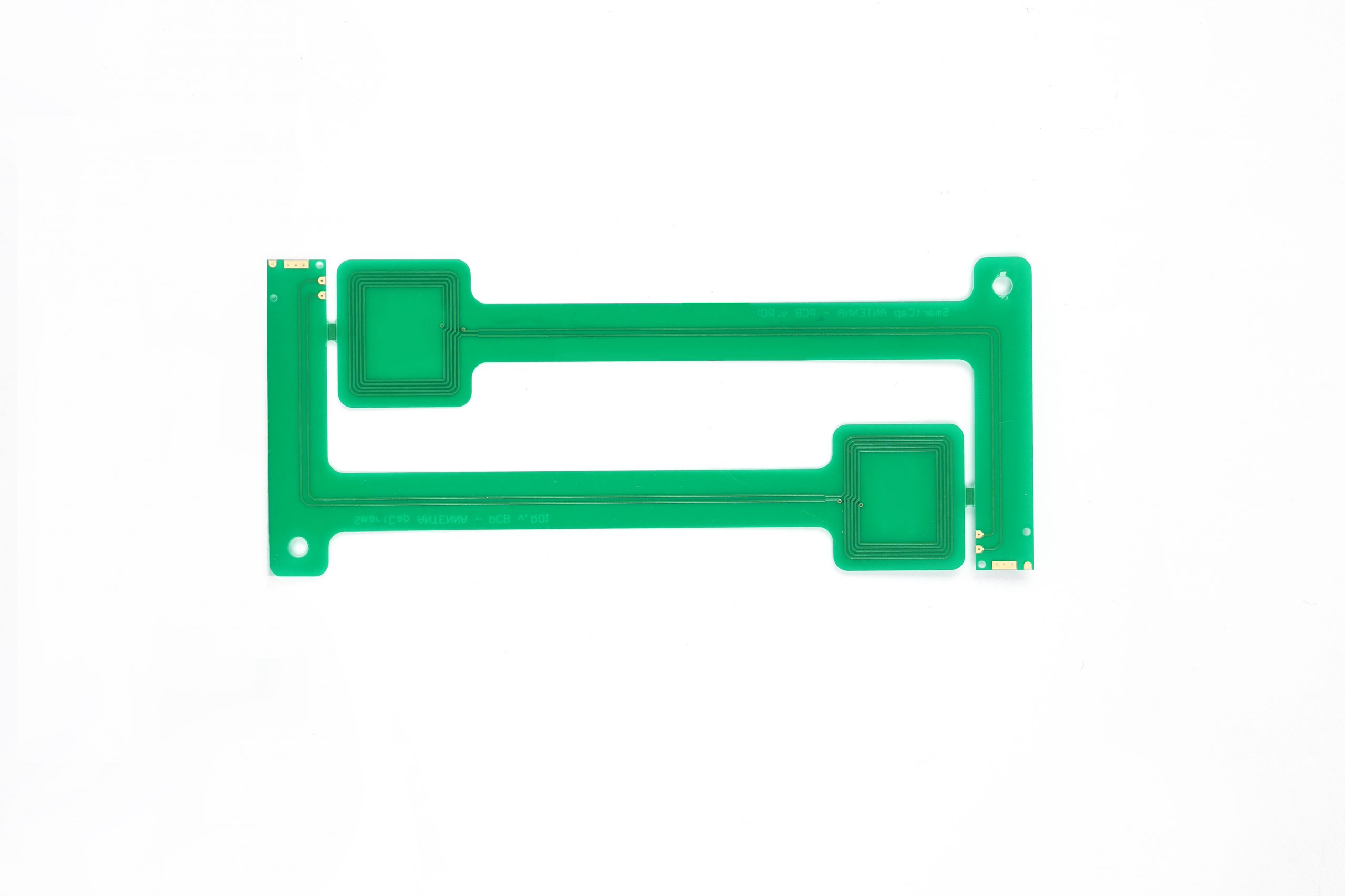
- Flexibility Adaptability: Extra Thin PCBs bend and conform to unconventional shapes, making them ideal for curved or foldable IoT products, from health monitors to flexible environmental sensors.
- Enhanced Thermal Performance: Advanced materials dissipate heat effectively even in thin layers, preventing overheating in densely packed IoT electronics during prolonged operation.
- High-Density Circuitry Support: Precision manufacturing enables complex multi-layer designs with fine traces, accommodating sophisticated IoT functionalities like wireless connectivity or data processing in tiny footprints.
- Durability Under Stress: Rigorous testing ensures resistance to vibration, bending, and thermal cycling—critical for IoT devices exposed to dynamic environments like industrial sensors or outdoor trackers.
- Power Efficiency: Optimized conductive paths minimize energy loss, extending battery life in IoT edge devices that require long-term, low-power operation.
- Cost-Effective Scalability: Streamlined production techniques make Extra Thin PCBs viable for mass-produced IoT solutions, balancing performance with affordability for consumer and industrial markets.
What Are the Applications of Extra Thin PCB in IoT?
Applications of extra thin PCB in IoT:
- Wearable Health Devices – Ultra-thin circuits embedded in skin patches for continuous vital sign monitoring
- Smart Home Systems – Paper-thin sensors hidden behind wallpapers detecting temperature/humidity changes
- Industrial Equipment Monitoring – Flexible vibration sensors conforming to machinery surfaces
- Precision Agriculture – Disposable soil sensors measuring moisture/nutrient levels across fields
- Pharmaceutical Tracking – NFC-enabled circuits printed directly on medication packaging
- Medical Implants – Biocompatible neural interfaces with sub-millimeter thickness
- Consumer Electronics – Foldable circuits enabling compact wearable designs
- Logistics Management – Ultra-lightweight tracking tags attached to shipping containers
- Environmental Sensing – Waterproof air quality monitors deployed in urban areas
- Automotive Systems – Flexible pressure sensors integrated into vehicle interiors
Can Extra Thin PCBs Handle High-Current in IoT Devices Without Overheating?
Yes, extra thin PCBs can handle high-current demands in IoT devices when designed with thermal management and material optimization. Below are actionable insights for ensuring reliability:
- Thermally Conductive Substrate Materials: Select advanced substrates like polyimide blends or ceramic-reinforced composites. These materials outperform standard FR-4 in heat dissipation, making them ideal for power-intensive IoT modules such as smart grid sensors or industrial gateways.
- Optimized Copper Layouts: Increase copper thickness (e.g., 2oz plating) and widen traces (0.5mm+) to reduce electrical resistance. This minimizes Joule heating in high-current paths, critical for battery-operated devices like robotic vacuum controllers.
- Strategic Thermal Via Placement: Deploy staggered microvia arrays to transfer heat from component-dense zones to external heat sinks. This technique prevents thermal saturation in edge computing devices processing real-time video analytics.
- Embedded Metal Core Technology: Integrate copper or aluminum inlays beneath power-hungry components (e.g., voltage regulators). This reduces thermal resistance by up to 40% in applications like electric vehicle charging stations.
- Intelligent Component Zoning: Isolate heat-generating elements (MOSFETs, inductors) from temperature-sensitive components (antennas, MEMs sensors). This prevents signal degradation in wearable medical patches and similar devices.
- Passive Cooling Enhancements: Design enclosure vents or heat-spreading fins for stationary IoT units (smart locks, security cameras). Active cooling remains optional but adds maintenance complexity.
- Adaptive Current Management: Implement firmware that dynamically adjusts power allocation during peak loads. This protects PCBs from thermal runaway in wireless charging pads for drones and robots.
- Iterative Thermal Simulation: Use computational tools (ANSYS Icepak, SolidWorks Flow) to model heat flow before prototyping. Adjust trace geometries and material stacks based on simulated hotspot data.
- Surface Finish Considerations: Choose ENIG plating over HASL for flatter surfaces, improving thermal interface material adhesion. This benefits compact IoT modules with dense component layouts.
- Rigorous Environmental Testing: Validate designs under extreme conditions (85°C/85% RH) to meet IEC 62368-1 standards. Document thermal margins to assure clients of long-term reliability in smart city infrastructure.
How to Prevent Signal Loss in Ultra Thin Circuit Boards for IoT Edge Devices?
Below are methods about how to prevent signal loss in ultra thin circuit boards for IoT edge devices:
- Choose Low-Loss Substrates: Use materials like liquid crystal polymer (LCP) or modified polyimide to minimize signal attenuation. These substrates maintain performance at high frequencies (e.g., 5G, Wi-Fi 6).
- Design Tight Impedance Control: Route high-speed traces (e.g., RF lines, USB 3.2) with precise geometries. Validate using simulation tools to ensure impedance matching (e.g., 50Ω for RF).
- Maintain Clear Spacing: Keep ≥3x trace-width gaps between high-speed signals and adjacent traces. Use guard traces or ground planes in dense layouts (e.g., smart agriculture sensors).
- Integrate Embedded Components: Add distributed capacitance via laminate materials to reduce power noise in edge computing modules.
- Optimize Via Design: Use ≤0.1mm laser-drilled microvias to minimize stubs. Stagger vias in multi-layer boards for cleaner signal transitions.
- Shield Sensitive Circuits: Apply copper foil or conductive coatings to RF enclosures. Prevent EMI in wireless modules.
- Shorten Critical Paths: Route clock lines and data buses directly between components. Avoid loops in real-time systems (e.g., drone navigation).
- Route Differential Pairs: Use tightly coupled differential pairs for high-speed interfaces (e.g., MIPI, PCIe). Match trace lengths to reject noise.
- Manage Heat Near Components: Place thermal vias under power-hungry chips (e.g., SoCs) to stabilize impedance and prevent timing errors.
- Test with Specialized Tools: Validate designs using Time-Domain Reflectometry (TDR) for impedance and Vector Network Analyzers (VNA) for RF performance.
How Do Ultra Thin Circuit Boards Enhance 5G IoT Performance?
- Compact mmWave Antenna Integration: Embed 5G millimeter-wave (mmWave) antennas directly into device housings using Ultra Thin PCBs. This eliminates external connectors, reducing signal loss by 15-20% in smart city infrastructure like traffic drones or AR glasses.
- Low-Loss Material for High-Frequency Signals: Use PTFE or ceramic-filled substrates to minimize dielectric absorption at 28GHz/39GHz bands. This ensures 99% signal integrity for industrial IoT sensors monitoring real-time machinery vibrations in factories.
- Embedded Copper Cores for Thermal Management: Dissipate heat from 5G power amplifiers (PAs) using thinner substrates with copper inlays. This reduces thermal throttling by 40% in base stations, maintaining peak speeds during video streaming or AI inference tasks.
- Laser-Drilled Microvias for High-Density Circuits: Enable 10+ layer designs with 0.1mm microvias to combine antennas, filters, and processors in a single package. This cuts latency by 25% in autonomous vehicle collision-avoidance systems.
- Conformal 3D Design for Aerial Deployments: Wrap flexible Ultra Thin PCBs around curved surfaces in drones or robots, placing antennas 30% closer to endpoints. This improves signal reception for agricultural drones mapping crops via 5G-connected cameras.
- Stripline Geometry for Reduced Insertion Loss: Lower insertion loss by 30% using stripline or coplanar waveguide (CPW) traces. This boosts SNR for AI-enabled surveillance cameras streaming 8K video over 5G networks.
- Lightweight Design for Extended Battery Life: Reduce device weight by 20-40% with thinner PCBs, enabling 50% larger batteries in 5G AR glasses. This supports 8+ hours of continuous connectivity for field technicians accessing cloud-based diagnostics.
How to Maintain Consistent Performance in Ultra Thin Circuit Boards for 5G IoT Networks?
- Select Thermally Stable Substrates: Use materials like liquid crystal polymer (LCP) or ceramic-filled PTFE with low coefficients of thermal expansion (CTE). This prevents warpage under 5G power amplifier (PA) heat, ensuring consistent impedance for mmWave signals in smart city gateways.
- Tighten Impedance Control Tolerances: Design traces with ±3% impedance tolerance using advanced electromagnetic simulation. This maintains signal integrity across -40°C to 105°C temperature swings in outdoor 5G IoT routers.
- Reinforce Microvia Durability: Deploy stacked microvias with electroplated copper fill and test for 1,500+ thermal cycles. Prevents via fracturing in 5G modules exposed to extreme environments like desert solar farms.
- Optimize Power Delivery Networks (PDNs): Integrate 01005-size decoupling capacitors and segment power planes to filter high-frequency noise. Stabilizes voltage rails for 5G baseband processors, reducing bit error rates (BER) during data bursts.
- Enhance Mechanical Robustness: Apply 50µm-thick ENIG (Electroless Nickel Immersion Gold) finish with 2µm gold thickness. Resists wear from 2,000+ mating cycles in industrial 5G edge computers with frequent connector changes.
- Implement Advanced Environmental Testing: Conduct 96-hour HAST (Highly Accelerated Stress Test) and 7-day salt spray testing. Identifies weaknesses in 5G agricultural sensors deployed in coastal regions with high humidity.
- Leverage Embedded Sensors for Real-Time Monitoring: Add onboard temperature/humidity/vibration sensors linked to edge AI. Enables predictive maintenance in 5G-enabled drones, alerting operators to thermal drift before it impacts video analytics.
- Improve Layer-to-Layer Registration: Use laser-aligned lamination processes to maintain ±10µm registration across 12+ layers. Prevents signal skew in 5G phased-array antennas requiring nanosecond-level timing accuracy.
- Adopt Hybrid Rigid-Flex Construction: Combine rigid PCB sections with flexible zones for vibration-prone applications. Reduces solder joint fatigue in 5G robotics controllers exposed to constant motion.
- Certify Component Suppliers for 5G Readiness: Audit capacitor/inductor vendors for AEC-Q200 compliance and 5G-specific testing. Ensures passive components withstand 5G’s 28GHz frequencies without parametric drift.
Conclusion
In conclusion, ultra-thin PCBs have become essential components for next-generation IoT devices, offering unparalleled space savings, superior signal integrity, and excellent thermal management. As demonstrated throughout this article, EBest Circuit (Best Technology)’s advanced manufacturing capabilities enable us to produce reliable 0.1-0.2mm ultra-thin boards with 15μm precision line spacing and <50ppm defect rates – ideal for wearables, medical implants, and 5G edge computing applications. Our proprietary thin-film deposition and copper-filled microvia technologies ensure your IoT products achieve maximum performance while avoiding signal loss or overheating issues. For cost-effective, high-quality ultra-thin PCB solutions that accelerate your IoT development timeline, contact EBest Circuit (Best Technology) today for a competitive quote and technical consultation. Let’s collaborate to bring your innovative IoT concepts to market faster and more reliably: sales@bestpcbs.com.