

Ever wondered why HASL finish PCB remains a cost-effective choice despite its limitations in high-density designs? This guide explores everything from HASL’s solder composition and pitch constraints to manufacturer selection criteria, while addressing thermal risks for heavy copper boards, RoHS compliance trade-offs, and main differences with ENIG finishes.
EBest Circuit (Best Technology) stands out as your trusted HASL surface finish PCB manufacturer by directly tackling the critical challenges faced by global buyers. We understand the frustrations of inconsistent quality, delayed deliveries, and hidden costs in cross-border procurement. Our HASL finish PCB are manufactured with IPC-A-600 Class 3 standards, ensuring reliable performance even in demanding environments like automotive and industrial applications. With 15-day standard lead time (30% faster than industry averages) and competitive pricing, we eliminate supply chain bottlenecks while keeping your budget intact. Every board undergoes 100% automated AOI testing to prevent defects like uneven coating or oxidation. Backed by 10+ years of experience serving EU/NA markets, we offer 1 piece MOQ for prototyping, and 24/7 English engineering support to streamline your sourcing process. Let’s turn your PCB procurement from a pain point into a competitive advantage, request a quote today: sales@bestpcbs.com.
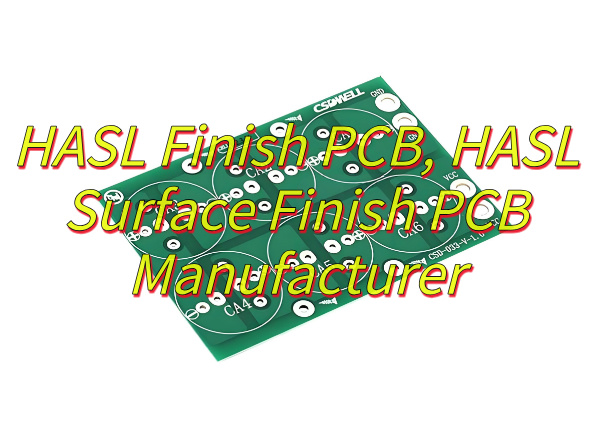
What Is HASL Finish PCB?
HASL Finish PCB (Hot Air Solder Leveling) is a common surface treatment for printed circuit boards, where molten solder (typically tin-lead or lead-free alloy) is applied to the copper pads and then leveled using hot air to create a smooth, protective coating. This process prevents oxidation, enhances solderability, and ensures reliable electrical connections during component assembly. While cost-effective and widely used, HASL finish may leave uneven surfaces unsuitable for fine-pitch components, leading to alternatives like ENIG or immersion silver in high-density designs. The method remains popular for general-purpose PCBs due to its durability and ease of inspection.
What Is the Composition of HASL Finish PCB?
Below are the compositions of HASL finish PCB:
- Solder Alloy: Solder alloys composed of tin (Sn) and lead (Pb) are mainly used, with a common ratio of 63% tin and 37% lead. However, due to environmental protection requirements and regulatory constraints such as RoHS (Restriction of Hazardous Substances Directive), lead-free solder alloys are now more common. These lead-free alloys are usually made of tin combined with other elements such as silver (Ag), copper (Cu) or bismuth (Bi), which can meet environmental standards and ensure soldering performance.
- Flux: Before the printed circuit board (PCB) is immersed in molten solder, the flux needs to be applied to the copper surface. Its main function is to remove oxides and contaminants on the copper surface, improve solder wettability, and enhance adhesion during soldering; at the same time, it can also prevent the copper surface from being oxidized again in subsequent steps, laying the foundation for high-quality soldering.
- Copper Substrate: The copper substrate is the basis of the HASL surface treatment PCB and undertakes the conductive function of the PCB. The HASL process is designed to protect the copper substrate from oxidation and corrosion, thereby ensuring the long-term stable operation of the PCB. In addition, the quality and thickness of the copper substrate also have an important impact on the overall performance of the HASL surface-treated PCB. Better copper materials and appropriate thickness can improve electrical performance and mechanical strength.
- PCB Base Material: In addition to the copper substrate, the base materials of the PCB (such as epoxy glass fiber boards such as FR-4) are equally important. These materials provide mechanical support and electrical insulation performance. Their quality, heat resistance, and flame retardancy will affect the reliability and service life of the PCB, and are also closely related to the adaptability of the HASL process.
- Protective Masking: Protective Masking can cover areas on the PCB that do not require soldering to prevent solder from accumulating in these areas. At the same time, it can further protect the circuit from environmental factors (such as moisture and dust) and improve the stability and durability of the PCB.
What Is the Minimum Pitch for HASL Finish PCB?
The minimum pad pitch for HASL finish PCB is not a fixed value. Generally speaking, it is difficult to achieve a pitch less than 0.5mm for standard HASL processes; in some cases, a well-calibrated HASL process with proper air knife control can achieve a minimum pitch of about 0.4mm.
Factors affecting pad pitch and solutions
Component – Dependent
- Impact: The minimum pitch for HASL surface finish PCBs depends largely on the components used. Larger through-hole components can have relatively wide pitches; however, fine-pitch surface mount components pose challenges for the HASL process.
- Solution: Choose the appropriate process based on the component type. For fine-pitch surface mount components, other more suitable surface finishes can be considered; if the HASL process must be used, communicate with the manufacturer in advance to optimize the process.
Process Variables
- Impact: Variables in the HASL process itself affect the minimum achievable pitch. The air knife angle and pressure used to level the solder are critical. Non-optimal air knife settings can result in uneven solder distribution and bridges between fine-pitch pads.
- Solution: Accurately calibrate the HASL process, tightly control air knife parameters, and perform multiple trials to find the optimal air knife angle and pressure settings to ensure uniform solder distribution.
Solder Alloy Characteristics
- Impact: The type of solder alloy used affects the minimum pitch. Lead-free solder alloys have different melting points and flow characteristics than traditional tin-lead alloys, requiring more precise control in the HASL process to achieve fine pitch. Some lead-free alloys are better suited for slightly coarser pitches, while others can be used for finer pitches after careful process adjustments.
- Solution: Choose the solder alloy appropriately based on the minimum pad spacing required. Perform process testing and adjust process parameters to suit the alloy characteristics before using a new alloy material.
How to Choose A Good HASL Surface Finish PCB Manufacturer?
Below are methods about how to choose a trusted HASL surface finish PCB manufacturer:
Experience & Reputation
Priority: Select manufacturers with >5 years of industry experience.
Verification Methods:
- Check Google Reviews and industry forums for customer feedback (focus on soldering inconsistency, board contamination issues).
- Confirm certifications: ISO 9001 (general quality management), ISO 13485 (medical devices), etc.
Quality Control
In-Process Inspection
- Require solder thickness test reports (standard: 0.8–1.5mil) using X-ray thickness gauges.
- Validate use of AOI (Automated Optical Inspection) for real-time defect detection (bridging, voids).
Final Inspection
- Demand IPC-A-600H Class II/III inspection reports at delivery.
- Key dimensional tolerances: ±0.05mm (critical dimensions).
Equipment & Technology
Nitrogen-Protected HASL Line: Reduces solder oxidation by >30%.
Adjustable Hot Air Knife:
- Wind speed range: 50–200m/s.
- Solder layer uniformity: CV ≤5%.
Solder Pot Temperature Profile: Standard fluctuation range ±2℃.
Regulatory Compliance
- EU Market: RoHS 2.0 certificate (lead content <1000ppm).
- Military Projects: IPC-6012 Class 3 compliance.
- Automotive Electronics: IATF 16949 certification.
Customization Capabilities
- Minimum Line/Space: 0.15mm/0.15mm (standard capability).
- Special Finishes: Support for hybrid processes (e.g., ENIG + HASL).
- DFM Analysis: Require customized Design for Manufacturability (DFM) reports.
Delivery Performance
- Standard Orders: ≤7 working days.
- Rush Orders: 3-day delivery (subject to capacity confirmation).
- On-Time Rate: ≥95% (last 3 months’ record).
Technical Support
- 24/7 DFM Review: Online accessibility for design feedback.
- FAE Team: Professional Field Application Engineers for soldering parameter optimization.
- Warranty: 3-year warranty + free failure analysis service.
Cost Management
- Tiered Pricing: Compare quotes for 50/500/5000 pcs batches.
- Hidden Costs: Clarify testing, tooling, and rush fees.
- Panelization: Choose manufacturers offering panelized production (reduces unit cost by 15–25%).
Why Does HASL Finish Cause Uneven Surfaces on Fine-Pitch PCBs?
- Solder Flow: In fine-pitch areas, narrow pad gaps and solder surface tension can cause uneven flow, leading to bridging between pads.
- Air Knife: Inconsistent air pressure or suboptimal angles across the PCB surface, especially in fine-pitch regions, can leave excess solder unevenly.
- Thermal Changes: Rapid heating and cooling during HASL can cause differential expansion and contraction in fine-pitch areas, warping the solder.
- Flux Residue: Unremoved flux residue acts as a barrier, causing uneven solder adhesion in fine-pitch areas.
- Complex Design: Boards with many fine-pitch components, multiple layers, and vias disrupt solder flow, making uniform finishes hard to achieve.
- Solder Alloy: Some alloys, particularly lead-free ones with high viscosity, struggle to flow smoothly in fine-pitch gaps.
- Process Variations: Minor fluctuations in temperature, solder bath composition, or conveyor speed accumulate and affect fine-pitch PCB surface quality.
Can Your HASL Manufacturer Prevent Thermal Damage to Heavy Copper PCBs?
Yes, EBest Circuit (Best Technology) has taken a series of strict and effective measures to prevent heavy copper PCBs from thermal damage during the HASL process. The specific implementation measures are as follows:
- Preheating Optimization: For heavy copper PCBs, EBest Circuit (Best Technology) will carefully optimize the preheating step. Before immersing the PCB in the molten solder bath, its temperature is gradually increased to reduce thermal shock. The preheating process is adjusted according to the thickness and copper content of the heavy copper PCB to ensure a more controlled temperature transition.
- Solder Bath Temperature Control: It is crucial to maintain accurate and stable solder bath temperature. EBest Circuit (Best Technology) is equipped with an advanced temperature control system that can accurately adjust the temperature of the molten solder to prevent the heavy copper PCB from overheating and causing thermal damage.
- Cooling Rate Management: After the HASL process is completed, the cooling rate of the heavy copper PCB is also critical. EBest Circuit (Best Technology) will use a suitable cooling system such as forced air cooling or temperature-controlled cooling chamber to control the cooling rate, slow down the cooling process, reduce the stress on the PCB, and avoid thermal damage caused by sudden temperature changes.
- Process Monitoring and Adjustment: Continuous monitoring of HASL process parameters is essential. EBest Circuit (Best Technology) deploys sensors and monitoring equipment to track variables such as temperature, air pressure, and conveyor speed in real time. Once any deviation is detected, the process is adjusted quickly to prevent thermal damage to heavy copper PCBs.
- Use of Thermal Protection Materials: In some cases, EBest Circuit (Best Technology) uses thermal protection materials or coatings on heavy copper PCBs before the HASL process. These materials help to dissipate heat more evenly and protect the PCB from excessive thermal stress.
- Customized Process Recipes: For heavy copper PCBs, EBest Circuit (Best Technology) develops customized HASL process recipes. These recipes take into account the specific characteristics of heavy copper PCBs such as copper thickness, number of layers, and board size to optimize the process and minimize the risk of thermal damage.
- Training and Expertise of Operators: Well-trained operators are key to preventing thermal damage. EBest Circuit (Best Technology)’s operators are familiar with the special requirements of heavy copper PCBs and can make real-time adjustments to the HASL process as needed. At the same time, the company conducts regular training and updates the latest technical knowledge to enhance the ability of operators to handle heavy copper PCB production.
- Testing and Validation: Before mass production of heavy copper PCBs with HASL surface treatment, EBest Circuit (Best Technology) conducts comprehensive testing and validation, including thermal cycle testing to simulate actual working conditions to ensure that the PCBs can withstand the thermal stress of the HASL process without damage.
Is Your HASL Finish RoHS-Compliant Without Sacrificing Solderability?
Yes, EBest Circuit (Best Technology) HASL finish RoHS-compliant without sacrificing solderability.
- Preheating Optimization: A good HASL manufacturer will carefully optimize the preheating step for heavy copper PCBs. By gradually raising the temperature of the PCB before immersion in the molten solder bath, it helps to reduce thermal shock. This preheating process can be adjusted based on the thickness and copper content of the heavy copper PCB to ensure a more controlled temperature transition.
- Solder Bath Temperature Control: Maintaining a precise and stable temperature in the solder bath is crucial. The manufacturer should have advanced temperature control systems that can accurately regulate the temperature of the molten solder. This helps to prevent overheating of the heavy copper PCB, which could lead to thermal damage.
- Cooling Rate Management: After the HASL process, the rate at which the heavy copper PCB cools is also important. A proper cooling system, such as forced – air cooling or a controlled – temperature cooling chamber, can be used to manage the cooling rate. Slowing down the cooling process can reduce the stress on the PCB and prevent thermal damage caused by rapid temperature changes.
- Process Monitoring and Adjustment: Continuous monitoring of the HASL process parameters is essential. The manufacturer should have sensors and monitoring equipment to track variables such as temperature, air pressure, and conveyor speed. If any deviations are detected, the process can be quickly adjusted to prevent thermal damage to the heavy copper PCB.
- Use of Thermal Protection Materials: In some cases, the manufacturer may use thermal protection materials or coatings on the heavy copper PCB before the HASL process. These materials can help to dissipate heat more evenly and protect the PCB from excessive thermal stress.
- Customized Process Recipes: For heavy copper PCBs, a manufacturer may develop customized HASL process recipes. These recipes take into account the specific characteristics of the heavy copper PCB, such as copper thickness, layer count, and board size, to optimize the process and minimize the risk of thermal damage.
- Training and Expertise of Operators: Well – trained operators are key to preventing thermal damage. The operators should be knowledgeable about the unique requirements of heavy copper PCBs and be able to make real – time adjustments to the HASL process as needed. Regular training and updates on the latest techniques can enhance their ability to handle heavy copper PCB production.
- Testing and Validation: Before mass – producing heavy copper PCBs with HASL finish, the manufacturer should conduct thorough testing and validation. This includes thermal cycling tests to simulate real – world operating conditions and ensure that the PCB can withstand the thermal stresses of the HASL process without damage.
What Is the Difference Between ENIG and HASL Finish PCB?
Here are difference between ENIG and HASL finish PCB:
Surface Finish Appearance
- HASL: Rough, uneven surface; traditional tin-lead HASL has non-uniform texture, lead-free may be matte.
- ENIG: Smooth, shiny surface with uniform nickel layer and reflective gold top layer.
Solderability
- HASL: Excellent; easily re-melted, reliable for soldering.
- ENIG: Good, but thick gold or nickel-gold interface issues can cause problems like “black pad”.
Cost
- HASL: Cost-effective; simple equipment and materials, lower alloy cost.
- ENIG: Expensive; specialized chemicals, complex equipment, costly materials.
Corrosion Resistance
- HASL: Some protection, but solder can oxidize in harsh conditions.
- ENIG: Better; nickel barrier and oxidation-resistant gold layer.
Compatibility with Components
- HASL: Good with most components, challenges with fine-pitch due to uneven surface.
- ENIG: Highly compatible with all component sizes, smooth surface aids precision.
Process Complexity
- HASL: Straightforward; dip in solder bath, level with air knives.
- ENIG: Complex; multiple steps, strict control of temperature, chemicals, and time.
Shelf Life
- HASL: Decent; stable but may oxidize in humidity.
- ENIG: Good; stable gold layer, maintains quality in proper storage.
Conclusion
In conclusion, through this blog, we’ve explored what HASL finish PCB is, its composition, minimum pitch capabilities, how to choose a reliable HASL finish PCB manufacturer, reasons for uneven surfaces on fine-pitch PCBs, prevention of thermal damage to heavy copper PCBs, RoHS compliance, and the differences between HASL and ENIG finishes. If you’re looking for high quality HASL finish PCB, please don’t hesitate to reach out to us at sales@bestpcbs.com for a quote. Looking forward to hearing from you!
You may also like
Tags: HASL Finish PCB