





A decorative LED PCB provides the electrical connections and precise LED mounting positions required for an illuminated airport map. EBest Circuit offers custom FR4 and aluminum PCB manufacturing, SMT and through-hole assembly, component sourcing, and project-specific testing. Board shapes, solder mask colors, and LED layouts can be customized from prototype verification through volume production.
Are you deciding between solder mask colors, PCB materials, or LED assembly methods for a decorative map? Uneven brightness, LED misalignment, flicker, and assembly defects can spoil the intended appearance and create costly rework. This guide explains the manufacturing requirements, material choices, assembly risks, and quotation inputs needed even when the Gerber files are not yet complete.
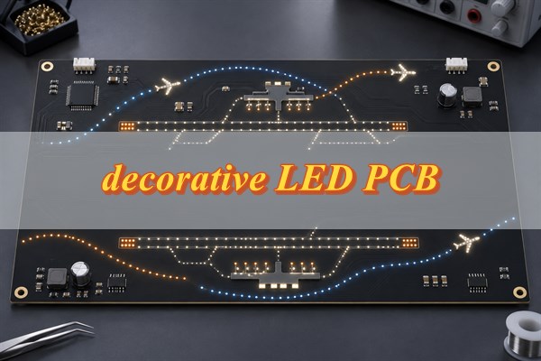
What Are Decorative LED PCBs Used for in Illuminated Airport Maps?
A custom decorative LED PCB can illuminate airport locations, flight routes, backlit graphics, and interactive features. The electrical architecture and LED arrangement should follow the visual function of the finished map.
- Airport location markers: Individual LEDs identify airports, cities, or destinations and must align with their corresponding map positions.
- Illuminated flight routes: LED groups form flight paths that can remain on, operate in groups, or illuminate sequentially when the control circuit supports that behavior.
- Backlit airport maps: LEDs illuminate outlines, labels, and graphic elements through acrylic panels, translucent materials, or optical diffusers.
- Interactive airport maps: Independently controlled LEDs or groups highlight selected destinations and routes.
- Aviation-themed displays: Custom LED boards can be integrated into wall displays, exhibition fixtures, and decorative products.
Large maps may use several interconnected PCB modules instead of one oversized board. This can simplify fabrication and installation, but connector placement, voltage drop, module alignment, and service access must be planned as one system.
What Are the Key Design Requirements for a Custom Decorative LED PCB?
The main design inputs are board thickness, copper weight, LED coordinates, mechanical dimensions, power distribution, and surface finish. Each choice must satisfy both the electrical design and the physical construction of the airport map.
- PCB thickness: Common FR4 options include 0.8 mm, 1.0 mm, and 1.6 mm. The final choice depends on board size, available installation space, support points, and connector requirements. Large, thin boards may need extra mechanical support.
- Copper thickness: Common nominal copper weights include 0.5 oz, approximately 17 µm, and 1 oz, approximately 35 µm. Trace width must reflect branch current, conductor length, acceptable voltage drop, and temperature rise.
- LED positioning: LED coordinates must match the airport locations or illuminated features. The PCB, placement data, artwork, and enclosure drawing should share one mechanical datum.
- Board outline and mounting: Shape, holes, cutouts, edge clearances, and connector orientation must match the panel or enclosure.
- Power and routing: The operating voltage and current depend on the chosen LEDs and driver. A 5 V, 12 V, or 24 V supply may be possible, but it is not interchangeable without redesigning the circuit and protection scheme.
- Surface finish: ENIG provides a flat solderable surface for many small LED footprints. OSP or lead-free HASL may also be suitable when compatible with the component and assembly process.
LED alignment deserves its own tolerance budget. If a decorative panel has a 3.0 mm opening and the visible illuminated feature is 2.0 mm in diameter, perfect centering leaves only 0.5 mm of radial clearance. PCB fabrication, component placement, and final installation errors all consume that allowance. Manufacturing files should therefore include the PCB drawing, LED coordinates, and installation requirements, not only Gerber data.
Which Solder Mask Color Is Best for a Decorative LED PCB?
White solder mask is generally useful when the PCB surface participates in light reflection, while black solder mask suits dark visual themes and exposed boards. The optical stack, not color preference alone, should decide the final option.
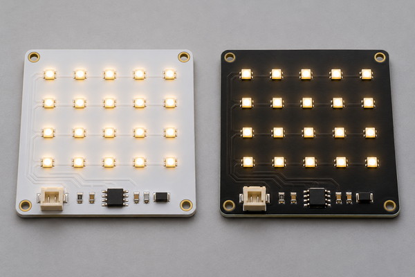
| Solder Mask Color | Main Characteristics | Typical Use |
|---|---|---|
| White | Higher visible-light reflectance; may improve light utilization in a compatible optical structure | Backlit maps and reflective LED lighting |
| Black | Dark appearance and relatively low visible-light reflection | Dark-themed maps and exposed decorative boards |
| Green | Conventional PCB appearance and broad process familiarity | Concealed boards without a special optical requirement |
| Blue, red, or another available color | Appearance tailored to a product concept, subject to process availability | Decorative products and branded visual designs |
Also specify whether the surface should be matte or glossy, whether white-mask color stability matters after soldering, and how solder mask registration will be controlled around small LED pads. When the light never interacts with the board surface, white mask may provide little optical benefit, so appearance and manufacturability should take priority. Confirm nonstandard colors and physical samples before locking the production files.
Which PCB Material Is Better for Decorative LED Lighting: FR4 or Aluminum PCB?
FR4 is usually the practical choice for distributed low-power LEDs and more complex routing. An aluminum PCB is more appropriate when concentrated LED power needs a shorter heat-spreading path.
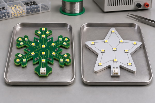
| Comparison | FR4 PCB | Aluminum PCB |
|---|---|---|
| Construction | Glass-reinforced epoxy laminate | Copper circuit, thermally conductive dielectric, and aluminum base |
| Common thickness options | 0.8, 1.0, and 1.6 mm are common examples | Depends on the selected metal-core construction |
| Thermal behavior | Can use copper area, thermal vias, and the mounting structure to improve heat transfer | Metal base spreads heat through the dielectric layer |
| Routing capability | Supports conventional multilayer routing and plated through-holes | A standard single-layer construction has more routing constraints |
| Main advantage | Flexible routing and familiar interconnection options | Better heat spreading for suitable LED loads |
| Typical fit | Distributed markers and control circuits | Higher-power or concentrated lighting zones |
Using LEDs does not automatically require a metal base. Thermal-dielectric conductivity values such as 1, 2, or 3 W/m·K describe the dielectric material under defined conditions, not the complete board-to-enclosure thermal path. Select the material after reviewing LED dissipation, routing complexity, ambient temperature, board size, and mounting contact.
Which Is Better for Decorative LED PCB Assembly: SMD or Through-Hole LEDs?
SMD LEDs are generally better for compact layouts and accurate automated placement. Through-hole LEDs are useful when a protruding lens must extend through a panel opening. Common SMD package designations include 0603, 0805, 1206, and 2835, while traditional round through-hole parts are often available in 3 mm and 5 mm formats.
Do not select a package by its family name alone. Confirm the exact mechanical drawing, light-emitting area, viewing angle, polarity, forward voltage, drive current, moisture sensitivity, and recommended land pattern in the chosen component datasheet. The official Lumileds LED datasheet library, for example, shows why package-specific documentation must be checked before the footprint and optical opening are approved.
- Component dimensions: Package height and lens position must fit the space between the PCB and decorative panel.
- Viewing angle: Narrow-angle devices concentrate light, while wider-angle devices can cover a larger optical area.
- Optical alignment: Align the actual light-emitting area, not only the nominal component center.
- Electrical compatibility: Forward voltage, current, polarity, and driver limits must match the circuit.
- Assembly route: SMD parts suit placement and reflow; through-hole parts need compatible insertion and soldering processes.
For a map with many small location markers, SMD assembly is normally more scalable. Use through-hole LEDs only when their lens geometry or mechanical retention provides a clear product benefit.
How Can You Achieve Uniform LED Brightness Across an Illuminated Airport Map?
Uniform brightness depends on controlled LED selection, stable branch current, low-loss power distribution, and consistent optical spacing. Assembly accuracy cannot compensate for an electrical architecture that allows large current imbalance.
- LED consistency: Use one approved part number and the required color or brightness bin for points that must look alike.
- Current control: Series-connected LEDs share one branch current; parallel branches need suitable current regulation or limiting components.
- Voltage drop: Check long power traces, connectors, and module-to-module wiring against the actual load.
- Switching behavior: Keep driver current loops compact, place decoupling correctly, and separate sensitive control signals from noisy power paths.
- Flicker: Define acceptable PWM frequency, current ripple, and camera-visible flicker when the display may be photographed or filmed.
- Optical spacing: Hold LED height, orientation, diffuser distance, and surface finish consistent across modules.
The driver topology must be evaluated with the chosen LEDs and branch arrangement. Texas Instruments’ application report on driving multiple LED strings illustrates that branch current depends on the feedback architecture, forward-voltage relationships, and resistor selection. A functional test should therefore define the supply condition, brightness-measurement method, allowable variation, and any flicker limit instead of checking only whether each LED turns on.
What Are the Main Challenges in Custom Decorative LED PCB Manufacturing and Assembly?
The main production risks are LED placement error, irregular board geometry, soldering defects, mechanical interference, and cosmetic variation. Each risk needs a corresponding drawing, process control, or acceptance criterion.
- LED misalignment: Wrong coordinates or orientation can shift a marker away from its map position. Use approved placement data and inspect critical locations.
- Irregular outlines: Complex contours, narrow sections, and internal cutouts can make panelization and separation harder. Define routing clearances, tooling support, and separation methods before release.
- Soldering defects: Poor pad geometry, stencil apertures, or reflow settings may cause insufficient solder, bridging, or component tilt.
- Mechanical interference: A connector, tall part, or misplaced hole can prevent installation behind the panel.
- Cosmetic defects: Scratches, stains, residue, or inconsistent mask appearance matter when the PCB remains visible.
Prototype approval should cover electrical operation, LED coordinates, mechanical fit, visible surface quality, and optical appearance under the actual panel. This prevents a board that passes an electrical test from failing the final display requirement.
How Are Custom Decorative LED PCBs Manufactured, Assembled, and Tested?
The workflow has six connected stages, from manufacturing-file review to application-specific functional testing.
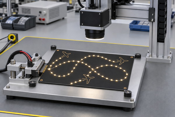
- Manufacturing file verification: Review Gerber data, drill files, outline, BOM, placement data, LED footprints, holes, mask openings, and connector positions.
- PCB fabrication: Manufacture the approved FR4 or aluminum construction using the applicable imaging, etching, drilling, surface-finish, solder-mask, profiling, and inspection steps.
- Component preparation: Verify LED and component part numbers, packaging, dimensions, polarity, and approved substitutions.
- SMT or through-hole assembly: Print solder paste, place SMD parts, reflow, and then complete any compatible insertion and through-hole soldering steps.
- Quality inspection: Electrically test bare boards for opens and shorts. Apply SPI, AOI, visual inspection, or another agreed method according to the assembly design and risk.
- Functional testing: Power the assembly under approved conditions and verify LED groups, connections, current behavior, and any specified brightness, color, or flicker criteria.
The purchase specification should identify which records are required, which test fixtures will be supplied, and what constitutes acceptance. “Functional test” is not a complete instruction unless the operating state and pass/fail limits are defined.
Project Inquiry: Custom Decorative LED PCB for an Illuminated Airport Map
The following is an illustrative preliminary-inquiry scenario, not a claim about a completed customer project. It shows how an airport-map concept can be translated into a quotation package before Gerber files are ready.
The buyer initially needs two answers: which solder mask colors are feasible and what information is required for a preliminary budget. To make that discussion useful, the supplier also needs the approximate board dimensions, outline, installation method, proposed LED type and count, preferred material, quantity, and assembly scope.
Challenge 1: Choosing a solder mask before the PCB design is complete.
The buyer can provide the map concept, intended visual theme, diffuser arrangement, and whether the PCB will remain visible. White and black samples may then be compared under the intended lighting. The final decision remains subject to the approved production files and available process options.
Challenge 2: Estimating cost with incomplete specifications.
A preliminary discussion can use an annotated drawing or PDF with overall dimensions, estimated LED count, material preference, quantity, and requested assembly. This produces a budgetary estimate, not a final manufacturing quotation.
Challenge 3: Avoiding mechanical redesign.
Check LED coordinates, mounting features, connector orientation, panel openings, and cable access against one mechanical drawing before the PCB files are released. Once Gerber, drill, BOM, and placement data are complete, a DFM review can identify fabrication and assembly concerns.
The output of this early stage is a list of missing decisions and quotation assumptions. No prototype performance, approved price, or production result should be claimed until the design and acceptance evidence actually exist.
Why Choose EBest Circuit for Custom Decorative LED PCB Manufacturing and Assembly?
EBest Circuit can coordinate bare-board fabrication, component sourcing, LED assembly, inspection, and agreed functional testing under one approved production package. The practical value is fewer file handoffs and clearer ownership of manufacturing questions.
- Material and finish review: Discuss FR4 or aluminum construction, surface finish, mask color, optical role, and installation conditions before release.
- Placement control: Manufacture and assemble to the approved LED coordinates, board outline, holes, and orientation data.
- Assembly-risk control: Use the appropriate SMT or through-hole process and agreed inspection points to identify polarity, placement, and solder-joint defects.
- Project-specific testing: Translate the buyer’s operating conditions into a documented functional test instead of relying on a generic power-on check.
- Revision control: Keep the approved PCB revision, BOM, placement data, and test requirements aligned for prototype and repeat orders.
- Early feasibility discussion: Review preliminary drawings before Gerber completion, followed by a free DFM check when manufacturing-ready files are available.
Capabilities, inspection records, and delivery documents should be confirmed for the specific order rather than assumed from a general service description.
What Information Is Needed for a Preliminary Decorative LED PCB Quote Without Gerber Files?
You can request a preliminary quotation with a dimensioned drawing and the information already known. A useful initial package includes:
- PCB dimensions: Estimated length, width, shape, holes, cutouts, and panel or enclosure constraints.
- Material: FR4, aluminum PCB, or an open request for thermal review.
- Solder mask: White, black, or another requested color, plus matte or glossy preference when appearance matters.
- LED information: Approximate quantity, package, color, brightness requirement, and coordinate arrangement.
- Electrical requirements: Supply voltage, current, control method, connector concept, and operating modes.
- Manufacturing scope: Bare board or complete PCBA with sourcing, SMT, through-hole assembly, programming, or testing.
- Order information: Prototype quantity, forecast volume, target delivery date, and destination.
An annotated airport map, PDF, or CAD drawing can support the budgetary review. Before fabrication starts, submit the approved Gerber or ODB++ data, drill files, stackup or material specification, BOM, placement file, assembly drawings, and test requirements.
FAQ About Custom Decorative LED PCB Manufacturing
Q1: Can customers specify LED brands or supply their own components?
A1: Yes. The exact manufacturer and part number may be nominated, or consigned parts may be supplied. Quantity, packaging, footprint, polarity, storage, and handling requirements must be checked before assembly.
Q2: Can a decorative LED PCB include custom logos or silkscreen markings?
A2: Yes, when the approved artwork and available print process support them. Markings must stay clear of pads, optical openings, and mounting features.
Q3: Does an indoor decorative LED PCB require conformal coating?
A3: Not necessarily. Evaluate coating only when moisture, dust, handling, or another environmental risk justifies it, and confirm compatibility with LED packages and optical surfaces.
Q4: How can exposed black or white PCB surfaces be protected during shipping?
A4: Use agreed visual inspection, suitable separation layers, antistatic packaging, and low-friction handling. Appearance-sensitive acceptance criteria should be written before production.
Q5: Can an alternative LED be used if the original part becomes obsolete?
A5: Yes, after reviewing package dimensions, land pattern, polarity, voltage, current, brightness, color, viewing angle, and reliability requirements. Any optical or electrical change requires buyer approval.
Q6: Can EBest Circuit sign an NDA before receiving design files?
A6: An NDA can be requested before confidential drawings, BOMs, artwork, or other project files are shared. Confirm the agreement scope and parties before disclosure.
Q7: Can inspection and test records be supplied with the shipment?
A7: Records can be arranged according to the purchase specification. Define the required document, sampling plan, test condition, and acceptance limit before manufacturing.
Q8: How is PCB revision consistency maintained for repeat orders?
A8: Repeat production should use the approved PCB revision, BOM, placement data, and manufacturing notes. Review and approve every design change or component substitution before the next build.
Q9: Can one large airport map use several smaller PCB modules?
A9: Yes. Modular boards can simplify fabrication and installation, but module alignment, connector pinout, cable length, voltage drop, and service access must be designed together.
Q10: Is a preliminary quotation the same as a production quotation?
A10: No. A preliminary quotation is based on assumptions and incomplete data. The production quotation should follow the approved manufacturing package, quantities, assembly scope, and test requirements.
Get a Custom Decorative LED PCB Quote from EBest Circuit
Uneven brightness, misplaced LEDs, and unclear acceptance criteria are easier to prevent before the files reach production. EBest Circuit can review the board construction, LED assembly approach, and manufacturing risks for your illuminated airport map.
Send your preliminary drawing or approved Gerber/ODB++ package, BOM, quantity, stackup, assembly requirements, firmware or programming needs, test requirements, delivery date, and destination to sales@bestpcbs.com. A complete RFQ helps separate budget assumptions from production-ready requirements and supports a more reliable DFM review.
You may also like



Tags: Custom LED PCB Manufacturing, Decorative LED PCB, Decorative LED PCB Assembly, Illuminated Airport Map PCB