





A wearable PCB connects the sensors, power supply and wireless electronics inside a body-worn device. A tracker with a flat, sealed housing may use a small rigid board. A hearing aid with a microphone and receiver at different angles may need a flexible interconnect. The first manufacturing decision is where the components must sit and which parts of the circuit, if any, must bend.
EBest Circuit manufactures and assembles rigid, flex and rigid-flex boards to customer-approved designs. For compact products, our engineering review connects bare-board decisions with assembly requirements, from the panel that carries a small board through reflow to the pads a test fixture must reach. For a review of your wearable PCB design and a project-specific quotation, contact sales@bestpcbs.com.
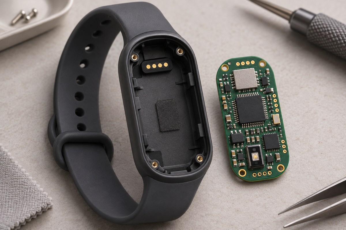
Wearable Electronics PCB Manufacturing at EBest Circuit
EBest Circuit supplies bare boards and assembled wearable electronics PCBs. On a tracker small enough to sit under a watch strap, the finished outline determines how the board fits the housing. The panel dimensions determine how it travels through assembly.
| Manufacturing Item | EBest Circuit Capability |
|---|---|
| FR-4 layer count, standard | 1–10 layers (high-Tg from 8 layers) |
| FR-4 board with a 5–10 mm side | Supplied in panel format |
| Standard FR-4 thickness, OSP or ENIG | 0.4–3.5 mm |
| Standard FR-4 thickness, HASL | 0.6–3.5 mm |
| Inner traces, 0.5 oz copper | 4/4 mil standard, 3/3 mil special |
| Outer traces, 1 oz copper | 4/4 mil standard, 3/3 mil special |
| Laser blind/buried via diameter | 0.10 mm, subject to stackup review |
| Minimum finished hole diameter | 0.20 mm standard, 0.15 mm special |
| All-flex PCB, one standard route | 1–4 layers, 0.06–0.60 mm finished thickness |
- Trace dimensions. The paired values give line width and spacing. Both depend on the copper weight on that layer.
- Stackup review. Layer count, finished thickness and via span must work in the same construction. Confirm the combination before releasing the layout.
- Assembly panel. Agree on the panel size separately from the single-board outline so the rails and tooling suit the assembly line.
Flexible PCB for Wearable Electronics: When to Choose Rigid, Flex or Rigid-Flex
Choose a flexible PCB for wearable electronics when the circuit must follow a fold or move during use. If all components fit on one fixed plane, a rigid board may be the simpler build even inside a curved enclosure.
| Comparison Item | Rigid PCB | Flex PCB | Rigid-Flex PCB |
|---|---|---|---|
| Typical fit | Flat module | Folded tail or moving strap | Modules on different planes |
| Component support | Rigid laminate | Local stiffeners where needed | Rigid component sections |
| Assembly concern | Panel separation | Carrier support during reflow | Fold alignment and transition clearance |
| Cost drivers | Layers and routing density | Stiffeners and tooling | Combined buildup and panel utilization |
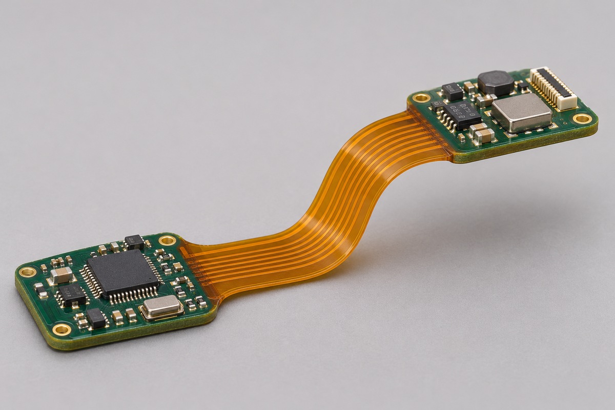
- One-time fold. A wearable flex PCB tucked behind a display bends during installation. Show the assembled shape, fold direction and available radius.
- Repeated motion. A flexible PCB for wearable devices that move with a strap needs a defined motion range and cycle requirement. Two circuits with the same flat outline can need different constructions.
- Connected modules. A wearable rigid-flex PCB can replace a separate connector between modules. Check the folded dimensions and component clearances before comparing its cost with two rigid boards and a cable.
HDI PCB for Wearable Devices: When Do You Need Microvias?
Consider an HDI PCB for wearable devices when conventional vias leave too little room to route signals out of the most crowded component footprint. Start with the package pad array and the layers those signals must reach.
- Check the escape path. A through via takes up space on every layer it crosses. A blind microvia can connect a surface pad to a nearby layer while leaving deeper layers free for routing.
- Compare fine lines with another buildup cycle. Finer traces may clear a short routing bottleneck. If several inner rows still have no exit path, review a microvia option against the copper weight and spacing available on the escape layer.
- Resolve via-in-pad details. Specify the via diameter and layer span. Where the via sits in a solderable pad, agree on filling and capping with the fabricator so the finished pad also suits assembly.
Wearable IoT PCB Requirements for Health Monitors and Trackers
A wearable IoT PCB must fit the sensor, battery and antenna in their operating positions. An assembled view helps the board supplier see constraints that are easy to miss in a flat layout.
- Sensor alignment. For an optical wrist monitor, check the sensor height against the enclosure window. For a hearing aid, check microphone orientation against the acoustic opening. A PCB manufacturer for wearable health monitors needs both the placement drawing and the mechanical tolerances to review that fit.
- Antenna clearance. When evaluating a wearable tracking device PCB manufacturer, ask how the antenna keepout and feed geometry will be preserved during fabrication. Nearby metal, the battery and the wearer can affect tuning. Review the 2.4 GHz PCB antenna manufacturing requirements and evaluate radio performance in the intended housing.
- Battery measurements. Leave fixture access to measure sleep current and radio activity before sealing the tracker. Define the operating state for each reading so the results can be compared across units.
Wearable PCB Design Checks Before Fabrication
A wearable PCB design review should resolve discrepancies between the electrical layout, the enclosure drawing and the assembly panel before tooling starts. Four checks have particular value on compact builds.
- Outline and height. Compare the finished outline and its tolerance with the housing pocket. Include the mounted height of the tallest component, solder joints and any stiffener or adhesive beneath the board.
- Connector access. A wearable PCB connector may fit on the layout while leaving no room to insert the flex tail or operate its latch. Check the insertion direction against the battery and housing wall in the assembled view.
- Bend and transition areas. Mark the bend location on the fabrication drawing. Review nearby vias, solder lands and stiffener edges against that location so the circuit bends where the mechanical design intends.
- Panel and separation method. Agree on rail positions, fiducials and breakaway tabs. A tab close to a small ceramic component or a sensor can put stress on the assembly during separation. Move the tab or revise the separation method while the panel is still on the drawing.
PCB Assembly for Wearable Electronics
PCB assembly for wearable electronics starts with keeping the board stable through paste printing, placement and reflow. Three decisions deserve attention before the first unit reaches the line.
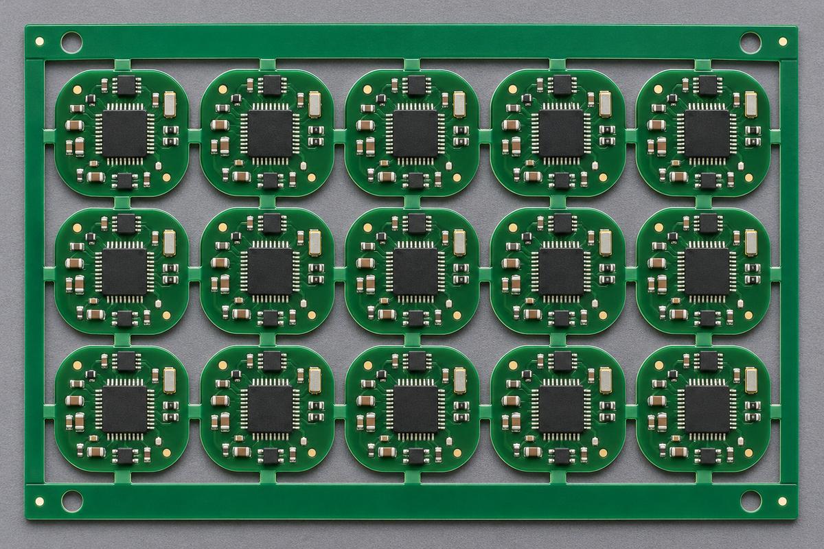
- Board support. A small rigid board can stay in its panel through assembly. Flex PCB assembly for wearable devices may require a carrier that supports component areas and leaves clearance for parts already mounted underneath.
- Placement orientation. Match the assembly drawing, BOM and placement coordinates by reference designator. A sensor rotated by 180 degrees can still fit its footprint. A visible pin-one mark and a drawing at the correct revision help catch that error before reflow.
- Sensitive components. PCB assembly for wearable health monitors may involve an optical window or a microphone port that needs protection during handling. Check the component supplier’s cleaning instructions when planning the stencil, fixture and cleaning process.
Wearable PCB Assembly Inspection and Functional Testing
For wearable PCB assembly, select each inspection method according to the defect or function it can detect. Agree on coverage and acceptance criteria before the build.
| Inspection Method | Inspection Focus | Applicable Stage |
|---|---|---|
| Bare-board electrical test | Netlist opens and shorts | Before assembly |
| Solder paste inspection | Deposit position and volume | After printing |
| Automated optical inspection | Visible placement and solder defects | After reflow |
| X-ray inspection | Hidden joints, including BGA joints | After reflow, as specified |
| Functional test | Startup, sensor response or sleep current | Assembled board with test firmware |
- Fixture access. Place circuit board test points where the fixture can reach the required rails and signals.
- Acceptance records. For a high-reliability wearable PCB project, define the firmware revision, test sequence, limits and results to record per unit or lot.
- Device validation. A board-level test can confirm that a sensor responds. Measurement accuracy on the body requires separate validation of the finished device.
What Drives the Cost and Lead Time of a PCB for Wearables?
For a PCB for wearables, the lowest bare-board unit price does not always give the lowest assembled cost. A rigid-flex design can cost more to fabricate yet remove a connector and a manual connection step. Compare both options at the same production quantity and test coverage.
- Fabrication cost depends on how many boards fit on a manufacturing panel, the layer buildup, the via process and any special tolerances. An irregular outline can use more panel area than its finished dimensions suggest.
- One-time costs can include a stencil, flex carrier, programming fixture or functional test fixture. Separate these charges from the recurring unit price, particularly when comparing a prototype lot with a repeat order.
- Lead time depends on the latest available input. A finished PCB cannot enter assembly until the approved sensor, connector and other required parts are available. Ask for fabrication, procurement, assembly and test milestones when a prototype date matters.
Why Choose EBest Circuit as Your Wearable Device PCB Manufacturer?
EBest Circuit can review the bare board and assembly as a single build. For a compact product, that lets the buyer resolve issues that cross supplier boundaries while the drawings can still change.
- Panel planning: Small-board delivery requirements can be reviewed alongside assembly rails and depaneling locations, so the quoted panel suits both fabrication and placement.
- Process selection: Distinguishing standard trace spacing from special processing gives the layout team a concrete choice between revising a local bottleneck and paying for tighter geometry.
- Construction review: Rigid, flex and rigid-flex options can be assessed against the same mechanical drawing. The comparison accounts for component support, connectors and assembly steps as well as board price.
- Assembly preparation: Reviewing the BOM, coordinates and assembly drawing together helps resolve orientation, package and material questions before the first build.
- Inspection planning: Visible joints, hidden joints and functional checks can be assigned appropriate inspection methods. The customer can define the required coverage and records before accepting a quotation.
How to Request a Wearable PCB Quote
Send EBest Circuit a fabrication package for a bare-board quote. For an assembled board, add the placement and test information so the quotation covers the product you intend to receive.
- PCB files: Gerber and drill data or ODB++, a dimensioned outline, stackup, finished thickness, copper weights, surface finish and impedance requirements where applicable.
- Mechanical details: An enclosure or folded view, component height limits, bend zones, stiffeners and critical tolerances.
- Assembly files: A BOM with manufacturer part numbers and approved alternatives, placement coordinates, an assembly drawing and any consigned-part details.
- Commercial and test scope: Prototype and repeat-order quantities, requested delivery date, programming requirements, test limits and the inspection records needed at delivery.
If the board construction is still open, identify the dimension or assembly step that is driving the decision. That gives the engineer a specific constraint against which to compare options.
FAQs About Wearable PCBs
Can I supply sensors or other critical components for assembly?
For a consigned build, include the manufacturer part numbers, available quantities, packaging and handling instructions. Agree on placement allowance and how unused parts will be returned.
Can the same panel be used for prototypes and production?
Often it can, provided the panel remains compatible with assembly equipment, test access and the separation method. Confirm before ordering repeat boards if the quantity or assembly route changes.
Should a sensor with the same footprint be accepted as a substitute?
Footprint compatibility is only one check. Review pin functions, firmware support, operating range and any calibration requirements, then obtain approval before substitution.
What should happen if the firmware changes after the pilot build?
Identify the firmware revision by lot or serial number and define which previously built units need reprogramming or retesting. Include the revision in the test record.
Can coating be applied around microphones, contacts or optical sensors?
Define keepout areas on the coating drawing and check the component supplier’s restrictions. An acoustic port, mating contact or optical window may need masking even when nearby circuitry is coated.
How should a bend-life requirement be specified?
Give the bend radius, angle, direction, number of cycles and electrical failure criterion. These conditions allow the fabricator and customer to agree on a representative test structure.
EBest Circuit handles both board fabrication and component assembly for wearable PCB projects. Reviewing the two together helps us spot details that affect the finished device, such as a connector that fits on the bare board but leaves too little room to operate its latch once the battery is installed. To discuss the board construction and assembly options for your next build, send your layout and enclosure drawing to sales@bestpcbs.com.
You may also like







Tags: HDI PCB for Wearable Devices, PCB Assembly for Wearable Electronics, wearable PCB