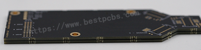
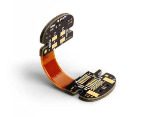
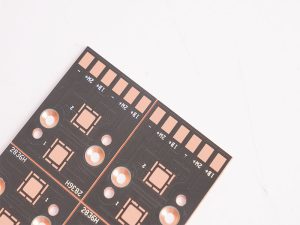
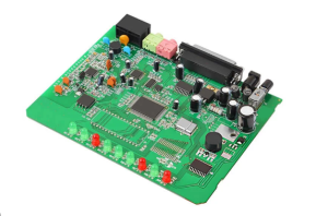
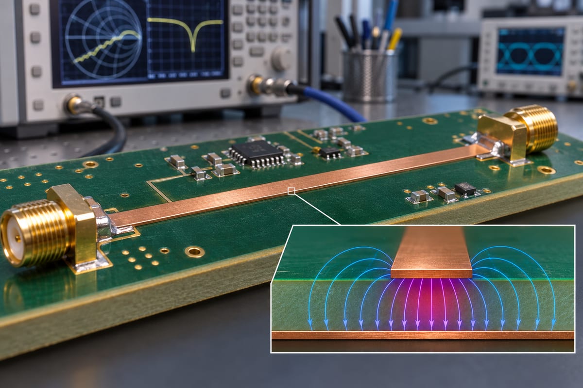
A microstrip is a planar transmission line with a conductor on an outer PCB surface and a reference plane separated by dielectric material. Keysight defines it as a thin conductive trace printed or etched on the top of an insulating substrate with a parallel ground plane on the other side. Because some electromagnetic field exists in air and some in the substrate, impedance and effective permittivity depend on both geometry and material.
How Does a Microstrip PCB Trace Work?
The signal and its return current form a transmission structure. At high edge rates or RF frequencies, the trace cannot be treated as an ideal wire. Its width, copper thickness, distance to the reference plane, dielectric properties and surrounding structures determine characteristic impedance, delay, loss and radiation.
Detailed Microstrip Design Parameters
| Parameter | Model input | Practical effect |
|---|---|---|
| Trace width | Finished top/bottom width or etch profile | Changes impedance and conductor loss |
| Copper thickness | Finished copper including plating where applicable | Changes cross-section and impedance |
| Dielectric height | Pressed distance to the reference plane | Strongly affects field spread and impedance |
| Material Dk/loss | Grade-specific design model at frequency | Controls delay, geometry and dielectric loss |
| Copper roughness | Model appropriate to foil/treatment | Can increase high-frequency attenuation |
| Solder mask | Thickness and dielectric behavior | Changes effective impedance for covered lines |
| Reference plane | Continuous geometry and openings | Controls return path and discontinuities |
Microstrip vs Stripline vs Coplanar Waveguide
| Structure | Field location | Strength | Trade-off |
|---|---|---|---|
| Microstrip | Outer layer, air and substrate | Easy probing and components | More exposed to radiation and environment |
| Stripline | Internal trace between planes | Better field containment | More vias and less direct access |
| Grounded coplanar waveguide | Outer trace with adjacent ground and lower plane | Useful field control and grounding | Gap, via fence and launch geometry become critical |
How Is Microstrip Impedance Calculated?
Use a field solver with the proposed production stackup rather than a single generic formula for sign-off. Closed-form equations are useful for early estimates, but real boards include copper thickness, trapezoidal etch, solder mask, roughness and anisotropic materials. For differential microstrip, pair spacing and symmetry also matter.
| Stage | Input quality | Output use |
|---|---|---|
| Early estimate | Nominal Dk and geometry | Choose layer and approximate width |
| Fabricator calculation | Actual laminate, pressed thickness and finished copper | Set production artwork and coupon |
| EM extraction | Launches, bends, vias and local structures | Analyze discontinuities and RF behavior |
| Coupon measurement | Controlled test structure | Verify the manufactured process |
Reference-Plane and Return-Path Rules
Keep a continuous reference plane beneath critical microstrip routes. Plane gaps, slots and poorly placed transitions force return current to detour, increasing loop area and potentially creating reflection, crosstalk and EMI. When a signal changes layers or reference planes, provide an appropriate nearby return connection based on the interface and stackup.
Nearby copper features also change the field. Ground pours, component pads, shields and board edges can alter local impedance when they sit inside the line’s field region. Define keep-outs or model the real copper instead of assuming an isolated textbook microstrip. The same review applies to differential pairs whose spacing changes near pads and connectors.
RF Launches, Bends and Via Transitions
A nominally correct straight line can still fail at connectors, pads, neck-downs, bends and vias. Model the launch as part of the channel. Miters or curved bends may reduce excess capacitance in some geometries, but the correct shape comes from the actual frequency and stackup. Ground-via placement and anti-pad geometry should be evaluated together with the signal transition.
Production Checklist

- Freeze material grade, dielectric thickness and copper construction.
- Use finished trace geometry and agreed etch tolerance.
- Document impedance target, tolerance, net class and test method.
- Keep the reference plane continuous below the line.
- Review solder-mask coverage and connector launches.
- Specify coupon design, location and report requirements.
- Recalculate after any material or stackup substitution.
Common Microstrip Failures
- Using a generic Dk rather than the laminate’s design value.
- Ignoring solder mask on a tightly controlled line.
- Routing across a reference-plane opening.
- Optimizing the trace while leaving the connector launch unmodeled.
- Measuring a coupon that does not represent the routed layer or geometry.
FAQ
Is every outer-layer trace a microstrip?
Only when it behaves as a transmission line referenced to an appropriate plane. Low-speed traces may not need transmission-line treatment, but the physical structure can still be microstrip-like.
Is microstrip always 50 ohms?
No. Fifty ohms is common in RF systems, but the target comes from the interface and system design.
Does a wider trace increase or decrease impedance?
With other inputs fixed, a wider microstrip generally lowers characteristic impedance. Recalculate the complete geometry rather than changing width alone.
When is stripline better?
Stripline is useful when field containment and reduced exposure are priorities and internal-layer routing is acceptable.
Sources
For a microstrip PCB stackup and manufacturability review, send fabrication data, material, frequency and impedance requirements to sales@bestpcbs.com. EBest Circuit can review manufacturing inputs; final RF performance remains subject to the customer’s design and validation.