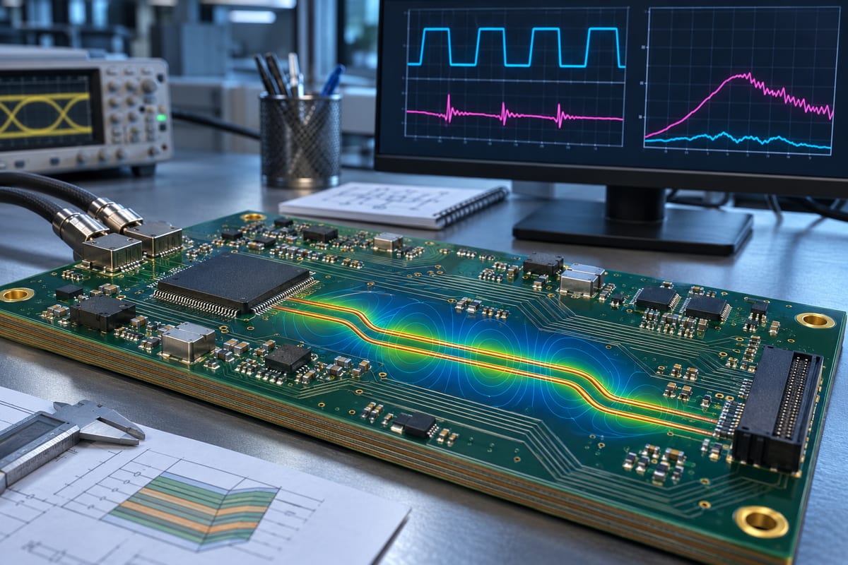
PCB crosstalk simulation estimates unwanted coupling from an aggressor interconnect into a victim interconnect. Useful results require more than drawing two parallel traces: the model must represent the production stackup, conductor geometry, coupled length, return path, vias, source behavior, receiver loading and the frequency or edge-rate range of interest. The simulation should answer a defined design question, such as whether induced noise violates a receiver threshold or reduces an eye-diagram margin.
What Is PCB Crosstalk?
Crosstalk is unintended electromagnetic coupling between nearby conductors. Changing voltage and current on the aggressor create electric and magnetic fields that induce a signal on the victim. Siemens identifies coupled length, spacing, stackup position, driver behavior and termination among the factors that control the result. Ansys similarly explains that dense routing can place traces close enough for unwanted coupling and recommends board-level analysis when routing rules alone do not establish adequate margin.
Near-end crosstalk (NEXT) is observed at the victim end near the aggressor source. Far-end crosstalk (FEXT) is observed at the opposite end. Their polarity and magnitude depend on the geometry, propagation behavior, termination and observation definition. Always label the ports and probing points in the report.
Detailed Simulation Parameters
| Input | What the model needs | Risk if simplified incorrectly |
|---|---|---|
| Stackup | Layer order, dielectric thickness, Dk/loss model and reference planes | Incorrect impedance, delay and field distribution |
| Copper geometry | Finished width, thickness, spacing and etch profile | Coupling and impedance do not represent production |
| Coupled length | Actual parallel run and changing separation | A short local coupling region becomes overstated or missed |
| Vias and transitions | Barrels, pads, anti-pads, stubs and return vias | Via-to-via and cavity coupling are omitted |
| I/O models | IBIS/SPICE/AMI or defined source and load behavior | Noise amplitude and timing use unrealistic edge strength |
| Termination | Source, parallel, differential or device termination | Reflections alter the observed crosstalk waveform |
| Analysis range | Time step, rise/fall time or frequency sweep | Relevant spectral content is not captured |
| Acceptance metric | Voltage, S-parameter, eye, jitter or receiver threshold | Plots are produced without a pass/fail decision |
Pre-Layout vs Post-Layout Crosstalk Simulation
| Approach | Best use | Model detail | Limitation |
|---|---|---|---|
| Pre-layout what-if model | Set spacing, layer and topology constraints | Representative stackup and parameter sweeps | Cannot include every final route and discontinuity |
| Post-layout extraction | Check actual aggressor/victim geometry | Routed traces, layers, vias and nearby structures | Quality depends on imported material and I/O data |
| 3D EM extraction | Dense vias, connectors, launches or nonuniform structures | Full electromagnetic geometry in a bounded region | Higher setup and computation cost |
| Bench measurement | Correlate prototypes and production channels | Physical coupons or completed boards | Measurement fixtures and calibration affect the result |
Altium’s documentation notes that its crosstalk analysis is post-layout because routed nets are required. Pre-layout simulation still has value for developing constraints, but final sign-off should incorporate the released geometry and applicable models.
Which Crosstalk Metrics Should Be Checked?
No single metric fits every interface. Time-domain NEXT and FEXT show induced voltage relative to switching events. Frequency-domain S-parameters quantify coupling versus frequency; mixed-mode terms are useful for differential pairs and mode conversion. Eye diagrams can show the combined effect of coupling, loss, reflections and timing, while jitter or receiver-mask measurements connect the channel result to protocol margin.
| Metric | Answers | Important condition |
|---|---|---|
| Peak NEXT/FEXT voltage | How large is the induced transient? | State driver pattern, edge rate, load and probe point |
| Coupling S-parameter | How does coupling change with frequency? | State port mapping, reference impedance and mode |
| Eye height/width | Does the combined channel preserve receiver margin? | Use correct data rate, pattern and receiver assumptions |
| Timing or jitter | Does aggressor activity move victim crossings? | Separate deterministic coupling from other jitter sources |
Crosstalk Simulation Workflow
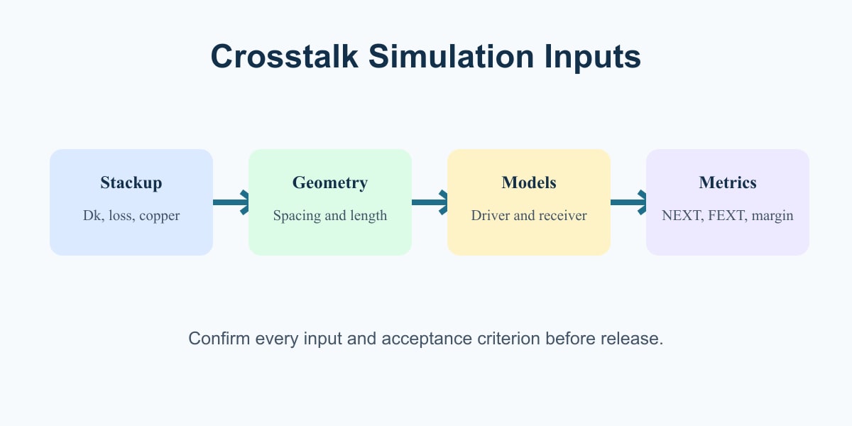
- Define the victim and aggressors. Include clocks, data, strobes, power-related switching and I/O routes that share a meaningful coupling region.
- Set the acceptance criterion. Use the interface’s receiver or system requirement rather than a universal spacing slogan.
- Import the production stackup. Confirm finished copper, dielectric thickness and relevant material models with the fabricator.
- Extract the actual geometry. Preserve spacing changes, reference-plane discontinuities, transitions and return vias.
- Assign electrical models. Use appropriate driver, receiver and termination behavior.
- Run useful cases. Sweep plausible process and geometry variation, not only a single nominal case.
- Identify the dominant mechanism. Separate trace-to-trace, via-to-via, cavity and common-mode contributions where possible.
- Change one design variable at a time. Compare spacing, layer, coupled length, reference placement, termination or via structure.
- Correlate high-risk channels. Use coupons, TDR, VNA or oscilloscope measurements with documented fixtures and calibration.
How Geometry Changes Crosstalk
Increasing separation generally reduces coupling, while longer parallel runs generally increase it. Moving a trace closer to a solid reference plane can contain more of its field, but the final effect depends on the complete geometry. Routing critical signals across plane gaps or close to I/O nets can create additional return-path and EMI problems. Differential symmetry also matters because imbalance can convert differential energy into common-mode noise.
A fixed “three-width rule” or similar spacing heuristic can be a conservative starting constraint, but it is not a universal pass condition. The acceptable spacing for a slow control line and a fast low-voltage memory interface may differ even on the same board. Simulation should use the actual edge spectrum and receiver margin.
Simulation vs Measurement: What Each Can Prove
Simulation isolates design variables and enables early sweeps before hardware exists. Measurement checks the physical realization, including fabrication variation and effects omitted from the model. Neither automatically validates the other. Correlation requires matching geometry, port locations, stackup, fixtures, terminations, stimulus and bandwidth. Siemens’ via-to-via crosstalk work demonstrates the value of comparing simulation with S-parameter and time-domain measurements on controlled test boards.
When results disagree, first audit input data and reference planes, then fixture removal, calibration, model bandwidth and material values. Do not tune an arbitrary parameter solely to force agreement without a physical explanation.
Common Modeling Mistakes
- Using nominal line width instead of the finished production geometry.
- Ignoring plane splits, voids, connector launches or via fields.
- Simulating frequency alone while the real risk is a fast edge with broad spectral content.
- Using ideal voltage sources when device output impedance and edge rate determine aggressor strength.
- Reporting NEXT or FEXT without port definitions and observation locations.
- Judging a color plot without a numerical acceptance criterion.
- Assuming a nominal pass covers dielectric, etch and registration variation.
FAQ
Do all PCB nets need crosstalk simulation?
No. Prioritize fast edges, low-noise analog victims, clocks, strobes, dense buses and routes with long close coupling or difficult transitions.
Is trace spacing enough to control crosstalk?
Spacing is important, but coupled length, reference structure, layer, edge rate, termination and vias also matter. Use spacing rules as constraints and simulation for risk-specific confirmation.
Should simulation use clock frequency or rise time?
Both context and edge behavior matter. A low repetition-rate signal can still contain high-frequency energy when its transitions are fast.
What fabrication data should be confirmed?
Confirm material model, pressed dielectric thickness, finished copper, trace/space tolerance, etch profile, via geometry and the final stackup used for impedance control.
Sources
- Ansys: PCB wiring and crosstalk design rules
- Siemens EDA: Crosstalk factors and simulation
- Altium: Configuring post-layout crosstalk analysis
- Siemens: Via-to-via crosstalk simulation and measurement
For PCB manufacturability and stackup review, send the released fabrication data, target stackup, controlled-impedance requirements, quantities and acceptance needs to sales@bestpcbs.com. EBest Circuit can review manufacturing inputs; system-level signal-integrity acceptance remains the customer’s design responsibility.