





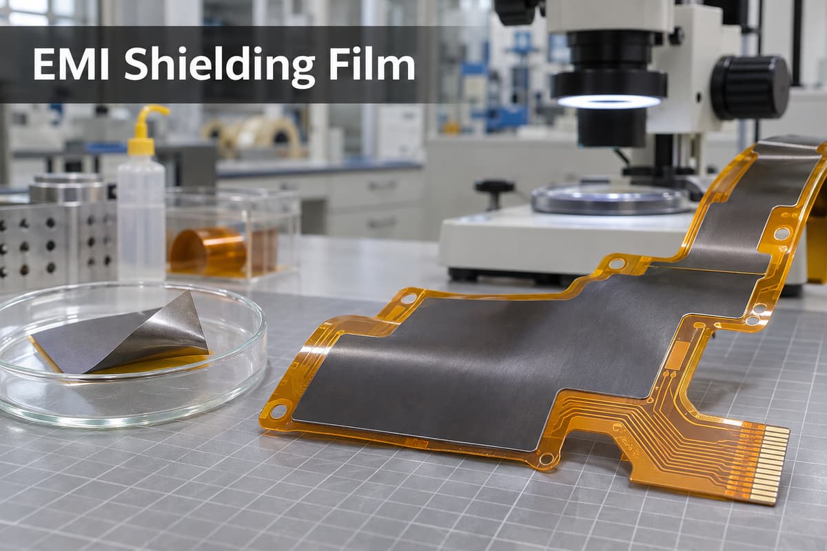
EMI shielding film is a thin multilayer material laminated onto a flexible printed circuit to reduce electromagnetic coupling while preserving a low-profile, bendable construction. It is not simply decorative metal foil. Its protective layer, shielding layer and conductive adhesive must form a controlled electrical and mechanical interface with the FPC.
Selection should start with the required frequency range, shielding target, total thickness, grounding method, bend condition and lamination process. A film that performs well on a flat test coupon can still fail after poor grounding, creasing, over-pressing or repeated dynamic bending.
What Is EMI Shielding Film?
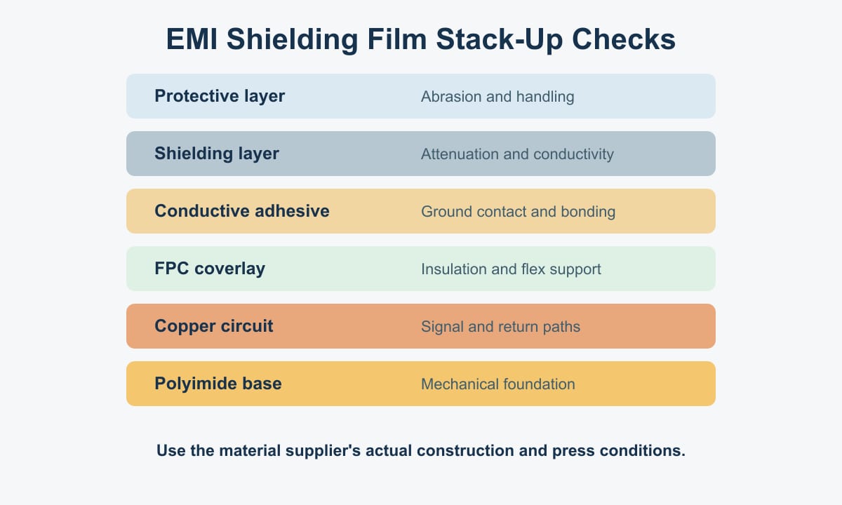
Shielding film for FPC commonly combines a protective surface, a conductive shielding layer and a conductive or anisotropic conductive adhesive. TATSUTA describes product families with thermosetting adhesive for FPC processing, pressure-sensitive versions for selected devices and supplementary grounding films. The exact construction varies by series, so design values must come from the selected supplier data sheet.
| Layer or feature | Primary job | Design risk |
| Protective layer | Handling and surface protection | Cracking, abrasion or excess stiffness |
| Shielding layer | Conductive path for field attenuation | Discontinuity, crease damage or inadequate frequency performance |
| Conductive adhesive | Bonding and electrical connection to ground features | High contact resistance or incomplete penetration |
| Release/transfer film | Processing support before lamination | Wrong removal sequence or contamination |
Detailed Film Parameters and Practical Meaning
As one product-specific example, TATSUTA’s SF-PC3900R1-C and R2-C sheet reports total pressed thicknesses of 12 µm and 13 µm, with shielding-layer thicknesses of 1 µm and 2 µm respectively. These are not universal values and must not be copied to another series.
| Parameter | What to verify | Why it matters |
| Total thickness after press | Finished laminate, adhesive flow and tolerance | Changes connector fit, bend stiffness and enclosure clearance |
| Shield effectiveness | Frequency, fixture, grounding and test method | A dB value without test conditions is not transferable |
| Contact resistance | Ground-pad geometry, pressure and aging | High impedance weakens the RF return path |
| Peel strength | Initial and aged adhesion to the actual coverlay | Delamination creates mechanical and electrical discontinuities |
| Press conditions | Temperature, pressure, time and release sequence | Controls adhesive flow, bonding and dimensional stability |
| Flex performance | Static bend or dynamic cycles, radius and direction | Film selection for a folding hinge differs from a fixed cable |
Shielding Film vs Copper Foil, Conductive Tape and Shield Cans
| Option | Best fit | Main trade-off |
| FPC EMI shielding film | Thin flexible circuits and folded assemblies | Requires controlled lamination and grounding |
| Copper foil with conductive adhesive | Local grounding, repair or simple shielding geometry | Can add stiffness and edge stress |
| Conductive fabric or tape | Conformable enclosure and gap treatments | Assembly consistency and long-term adhesion |
| Board-level shield can | Rigid PCB component regions | Height, soldering, seams and rework |
Grounding Design Rules
- Define where the film connects to the FPC ground rather than assuming full-area contact.
- Use the supplier’s recommended exposed-ground geometry and press construction.
- Keep the return path short and distributed where high-frequency performance requires it.
- Do not bridge a true isolation barrier with shielding film or grounding features.
- Check connector shells, chassis contacts and cable exits as part of the complete shield path.
- Measure contact resistance after lamination and after environmental or flex testing.
Lamination and Assembly Process
- Verify material identity, storage condition and shelf-life requirements.
- Clean and inspect the FPC coverlay and exposed grounding regions.
- Align the film without wrinkles, trapped contamination or unintended overlap.
- Apply the supplier-specified temperature, pressure and time.
- Remove transfer film in the correct sequence and inspect edges and apertures.
- Measure dimensions, adhesion and ground continuity before final assembly.
Pressing parameters are a material-system requirement, not a universal FPC recipe. Excessive pressure can distort fine features or force adhesive into unintended areas; inadequate pressure can leave weak bonding and unstable contact.
Bend and Mechanical Design Checks
Keep abrupt film edges, grounding transitions and thickness steps away from the highest-strain bend zone. Evaluate the full laminated stack, not the base polyimide alone. Static installation bends and repeated dynamic flex require different evidence. Define bend radius, flex direction, cycle count, temperature and fixture geometry, then inspect resistance and shielding performance after testing.
Common Failures and Root Causes
| Failure | Possible cause | Verification |
| Weak shielding | Poor ground contact, wrong film or uncontrolled aperture | Frequency-specific test and ground-resistance check |
| Delamination | Contamination, wrong press cycle or incompatible coverlay | Peel and environmental testing |
| Cracking at bends | Film too stiff, radius too small or edge in strain zone | Section inspection and flex cycling |
| Connector fit problem | Finished thickness not included in tolerance stack | Measure pressed stack and mating geometry |
| Intermittent noise | Ground contact changes during movement | Monitor resistance and RF behavior while flexing |
Validation Checklist
- Confirm film series, lot and storage history.
- Document final thickness and dimensional change after pressing.
- Measure grounding continuity and contact resistance.
- Inspect film edges, apertures, wrinkles and adhesion.
- Run bend testing that represents the final product motion.
- Test emissions or susceptibility with the final cables, enclosure and operating modes.
- Record the exact fixture, frequency range and acceptance limit.
FAQ
Can EMI shielding film be used on a rigid PCB?
Conductive films and tapes can be used in rigid assemblies, but FPC shielding film is optimized around flexible-circuit construction and lamination. Confirm compatibility with the actual surface and process.
Does thicker shielding film always work better?
No. Shielding depends on material, frequency, grounding, apertures and test conditions. Extra thickness can reduce flexibility and create mechanical problems.
Where should shielding film connect to ground?
Use defined exposed grounding features and the film supplier’s recommended construction. The connection must remain low impedance after pressing, bending and environmental exposure.
Can shielding film cross a dynamic bend?
Only when the selected film and complete FPC stack are qualified for the required bend radius, direction and cycle count. A static-fold product is not proof of dynamic-flex life.
Sources
- TATSUTA — EMI shielding film lineup and application guidance
- TATSUTA — SF-PC3900R1-C/R2-C product data
- 3M — EMI management and conductive adhesive guidance
For a flexible PCB stack-up, shielding-film opening and assembly review, send the controlled drawing, selected material series, bend requirements and validation targets to sales@bestpcbs.com.
You may also like

Tags: conductive shielding film, emi shielding film, flexible pcb emi, fpc shielding film