A custom traction inverter PCB needs reliable fabrication, an assembly process suited to its components and engineering support that keeps production aligned with the design. EBest Circuit provides custom PCB manufacturing and assembly for control, sensing and gate-driver interface boards used in traction inverter development.
With high-Tg multilayer fabrication, component sourcing, SMT and THT assembly, and inspection support, EBest Circuit helps you coordinate the transition from PCB files to assembled boards. Send your design files and quantity to sales@bestpcbs.com for a manufacturing review and quotation.
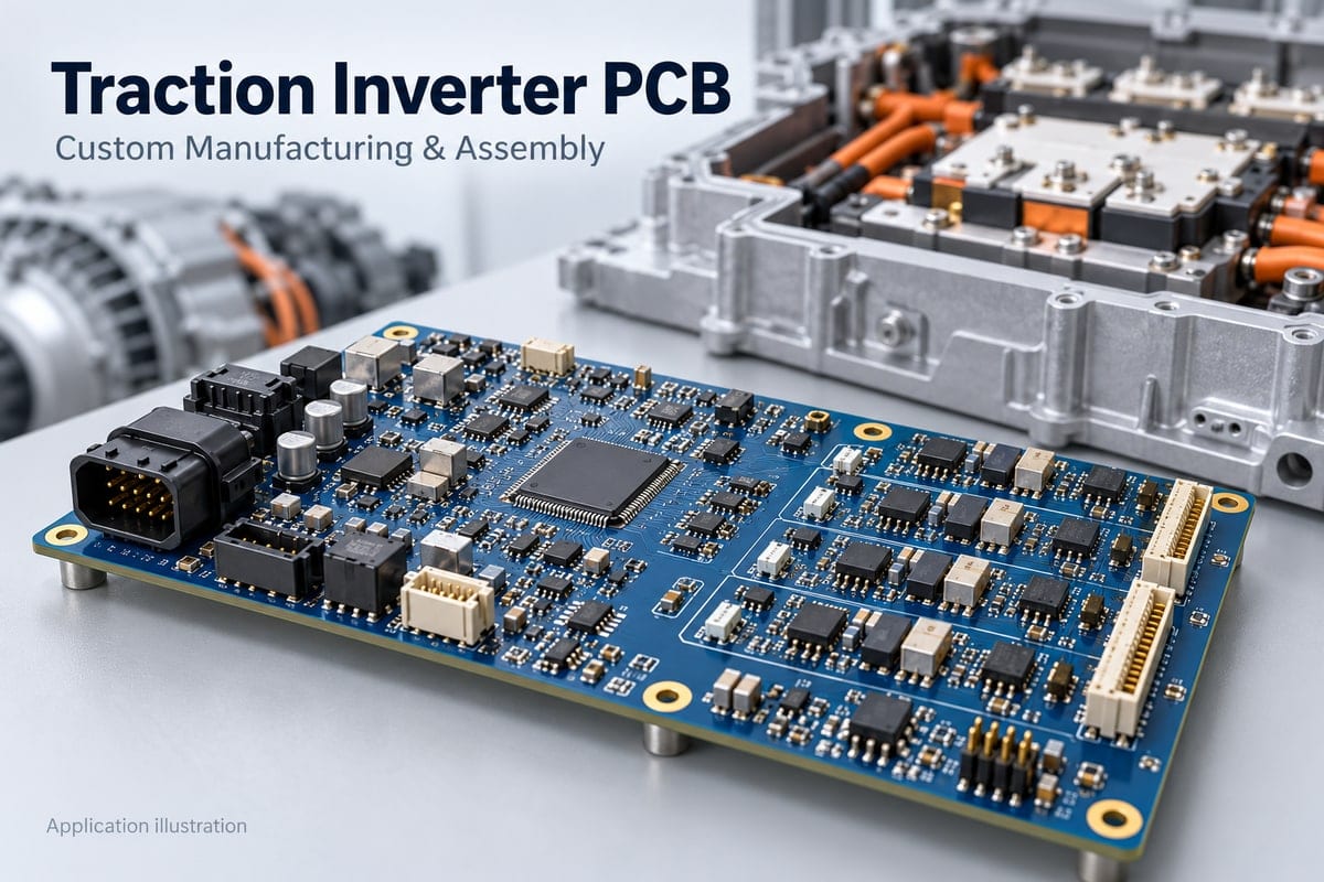
Traction Inverter PCB Types Manufactured by EBest Circuit
EBest Circuit manufactures boards to your design, matching the materials, copper construction and assembly process to each board’s function.
- Control PCBs — Multilayer construction supports processors, communication interfaces and mixed-signal circuitry. Stackup review helps accommodate dense routing, reference planes and the required finished thickness.
- Gate-Driver and Driver-Interface PCBs — Fabrication preserves specified isolation boundaries, compact driver connections and local supply routing. Copper geometry, solder-mask openings and component clearances receive particular attention.
- Sensing and Feedback PCBs — Boards for current, voltage and temperature feedback benefit from accurate conductor patterns, controlled assembly and cleanliness around sensitive measurement circuits.
- Auxiliary Power and Interface PCBs — Copper weight, plated holes and connector mounting are matched to local power distribution and interconnection requirements.
Each board is specified for its own electrical and mechanical duties. This keeps fabrication choices relevant to the application instead of applying the same construction across the entire inverter.
Custom Traction Inverter PCB Manufacturing Capabilities
EBest Circuit offers multilayer FR-4 fabrication with high-Tg materials, heavier copper, controlled impedance and blind or buried via options. The following parameters provide a starting point for evaluating your design.
| Manufacturing Parameter | Standard Process Range | Special Process Options |
|---|---|---|
| FR-4 Layer Count | 1–10 layers | 10–32 layers, subject to construction review |
| Inner-Layer Copper | 0.5–5 oz | 5–20 oz |
| Outer-Layer Copper | 1–5 oz | 5–20 oz |
| High-Tg FR-4 | Tg 170–180°C material options | Additional grades subject to material and process review |
| Board Thickness for ENIG | 0.4–3.5 mm | Thinner or thicker constructions evaluated individually |
| Minimum Finished Hole Diameter | 0.20 mm | 0.15 mm |
| Maximum Through-Hole Aspect Ratio | 8:1 | 10:1 |
| Inner-Layer Trace/Spacing at 2 oz Copper | 6/6 mil | 5/5 mil |
| Outer-Layer Trace/Spacing at 2 oz Copper | 8/8 mil | 6/6 mil |
| Surface Finish Options | ENIG, OSP, HASL, immersion silver, immersion tin and ENEPIG | Selected according to assembly and contact requirements |
Capability limits depend on the complete board construction. Copper weight, spacing, hole size and board thickness are reviewed together; their individual limits are not automatically available in the same design. Early review helps retain critical features without adding unnecessary process complexity.
PCB Materials and Stackup Options for Traction Inverters
EBest Circuit reviews material and stackup choices against your board’s thermal, insulation, routing and assembly requirements. Available high-Tg FR-4 options include grades such as S1000-2 and IT180, with the specific laminate agreed before production.
| Material or Construction Option | Suitable Application | Manufacturing Focus |
|---|---|---|
| High-Tg FR-4 | Control and interface boards requiring a specified laminate for assembly and thermal conditions | Material grade, finished thickness and compatibility with the assembly process |
| Higher-CTI Material Options | Boards with insulation barriers where tracking resistance influences the design | Material CTI, creepage requirements and availability of the specified grade |
| Four-Layer Stackup | Control, sensing and driver-interface boards with moderate routing density | Signal routing, reference-plane arrangement and copper balance |
| Higher-Layer-Count Stackup | Dense processors, multiple interfaces and complex power distribution | Layer registration, dielectric construction and via structure |
| Heavier-Copper Construction | Local supply distribution and conductors requiring greater cross-section | Copper-dependent spacing, etching allowances and soldering behavior |
Material selection and stackup planning work together. Tg alone does not establish continuous operating temperature or insulation capability. Where controlled impedance is required, EBest Circuit can review production dielectric thicknesses and conductor geometry before fabrication.
DFM and Layout Support for Traction Inverter PCBs
EBest Circuit’s DFM support focuses on resolving manufacturing issues before they become production delays. Engineering questions connect the supplied layout with the proposed fabrication and assembly processes.
- Copper Geometry Review — Checks trace widths and spacing against the selected copper weight, helping avoid features that become difficult to reproduce after etching.
- Drill and Via Review — Evaluates finished hole sizes, annular rings and thickness-to-hole relationships to identify plating and interconnection concerns.
- Isolation Features and Slots — Reviews the manufacturability of specified gaps, routed slots and copper keepouts while preserving the design’s electrical boundaries.
- Solder-Mask and Pad Review — Checks openings, mask bridges and via treatment around component pads to support consistent solder-paste deposition and assembly.
- Stackup and Panel Review — Coordinates finished thickness, layer construction, tooling features and panel support with fabrication and component placement.
Changes affecting electrical behavior are returned for design approval. This gives your engineering team visibility into proposed adjustments while allowing manufacturing questions to be resolved before production release.
Traction Inverter PCB Assembly Services
EBest Circuit combines PCB fabrication and assembly support so board construction, components and inspection requirements can be managed within one project.
- Component Sourcing — Procurement follows the agreed BOM, with component questions and proposed substitutions raised for approval. This helps align purchasing with the intended circuit and package requirements.
- SMT Assembly — Supports surface-mount control, sensing and driver-interface circuitry. Stencil preparation and reflow planning account for component size, pad design and copper distribution.
- THT Assembly — Supports through-hole connectors and other leaded components, with attention to hole fit, solder access and mechanical mounting requirements.
- Mixed-Technology Assembly — Coordinates SMT and THT operations for boards combining compact electronics with larger connectors or supporting components.
- AOI and X-Ray Inspection — Provides inspection of visible assembly features and, where appropriate, hidden solder joints according to the agreed inspection plan.
- Functional Testing Support — Testing can be scoped around customer-defined fixtures, firmware, interfaces and acceptance limits to assess the required board functions.
Coordinating these services helps resolve fabrication and assembly interactions early, including panel handling, connector access and the soldering demands of heavier copper.
Quality Control and Testing for Traction Inverter PCBs
EBest Circuit aligns inspection with the board construction and assembly requirements. Each method addresses a specific manufacturing concern.
- PCB Dimensional and Construction Checks — Verify relevant features such as finished thickness, conductor geometry, plated-hole copper and surface finish against the manufacturing specification.
- Bare-Board Electrical Testing — Checks circuit connectivity to identify opens and shorts before components are installed.
- Automated Optical Inspection — Examines visible component placement, polarity and solder-joint features to help detect assembly defects.
- X-Ray Inspection — Supports evaluation of hidden solder connections where package construction limits optical access.
- Cleanliness Inspection — Checks for solder balls, debris and unwanted residues, particularly around sensitive circuits and isolation regions.
- Agreed Functional Tests — Evaluate specified circuit functions using defined conditions and acceptance criteria.
Manufacturing inspection and application qualification serve different purposes. Insulation, environmental and system-level validation requirements should be defined for the intended application so the production and test scope can support them.
Custom Traction Inverter PCB Manufacturing Case Study
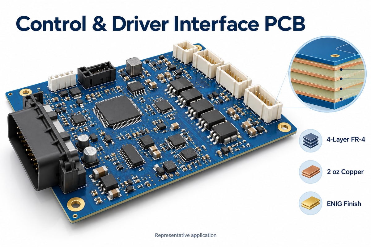
Application: A representative traction inverter control and gate-driver interface board combines PWM interfaces, sensing connections and local supply distribution near the power stage. The following application example uses an actual EBest Circuit four-layer PCB specification, with the construction matched to this engineering scenario.
Manufacturing Challenges:
- Heavier copper alongside compact circuitry. The 2 oz copper construction requires suitable etching allowances to preserve conductor widths and spacing around smaller components.
- Consistent plated-hole construction. The specified minimum hole-wall copper thickness of 25 μm requires attention to drilling, plating and verification.
- Different soldering demands across the board. Larger copper areas draw heat away from pads differently than smaller signal features, affecting solder-paste and reflow preparation.
EBest Circuit’s Solutions: The selected construction uses S1000-2M FR-4 with Tg170, four copper layers and a finished thickness of 1.6 mm ±10%. For this application, DFM review would check fine features against the 2 oz process and coordinate the stackup and panel before fabrication. Drill and plating planning would address the hole-wall copper requirement, followed by bare-board electrical testing.
ENIG provides a flat surface for component attachment. Assembly preparation would account for the copper distribution and component thermal mass, with AOI, X-ray and cleanliness checks included in the corresponding assembly requirements.
Customer Benefits: This approach connects copper geometry, plated-hole quality and soldering behavior in one manufacturing plan. It helps reduce avoidable fabrication and assembly rework while providing an inspectable board platform for inverter integration and testing. The four-layer construction also offers routing flexibility without introducing a more complex HDI structure solely for this representative application.
PCB Specifications:
| PCB Parameter | Selected Specification |
|---|---|
| PCB Type | Rigid multilayer FR-4 PCB |
| Application | Traction inverter control and gate-driver interface board — representative application |
| Layer Count | 4 layers |
| Base Material | S1000-2M FR-4, Tg170 |
| Board Thickness | 1.6 mm ±10% |
| Finished Copper Thickness | 2 oz on inner and outer layers |
| Surface Finish | ENIG; gold 1 μin, nickel 100 μin |
| Minimum Hole-Wall Copper Thickness | 25 μm |
| Solder Mask / Legend | Blue solder mask / white legend |
| Inspection Requirements | Bare-board electrical testing; AOI and X-ray for the corresponding assembly |
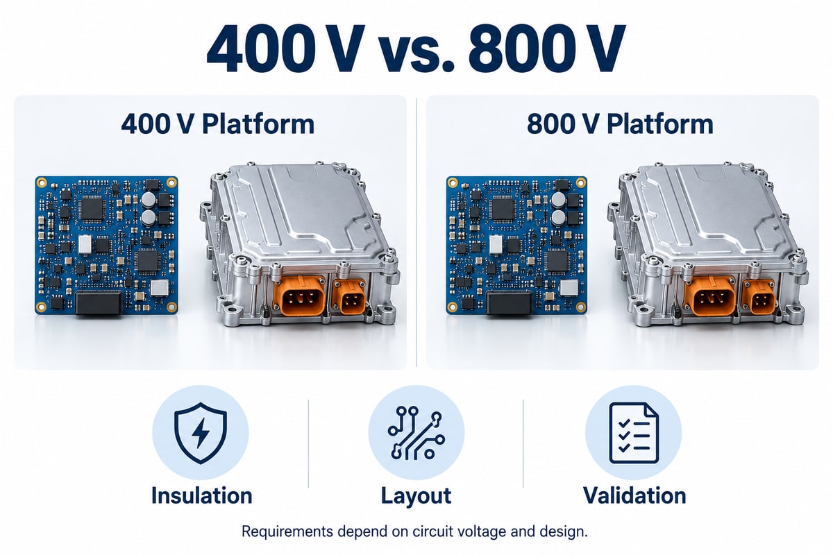
400 V vs. 800 V Traction Inverter PCB Requirements
The voltage across each circuit and isolation barrier determines the relevant PCB requirements. Moving to an 800 V platform does not automatically mean doubling every clearance or increasing copper thickness throughout the board.
| Design Consideration | 400 V Traction Inverter Platform | 800 V Traction Inverter Platform |
|---|---|---|
| Voltage Specification | Establish maximum operating voltage and transients for each circuit | Reassess circuit and barrier stresses for the higher-voltage platform |
| Creepage and Clearance | Derived from insulation requirements, material and environment | Often more demanding where the higher voltage appears across a barrier |
| Material Evaluation | Assess thermal properties, CTI and dielectric construction | Recheck these properties against the revised insulation requirements |
| Gate-Driver Layout | Depends on switching devices, edge rates and driver architecture | Fast-switching designs can place greater demands on parasitic coupling and return-path control |
| Voltage Sensing | Divider ratings, spacing and measurement range match the monitored voltage | Divider construction and component voltage distribution may require revision |
| Copper Thickness | Determined by local current and allowable temperature rise | Still determined by local current and temperature rise; voltage alone does not require thicker copper |
| Validation | Test against defined circuit and insulation requirements | Update test conditions and acceptance limits for the revised design |
EBest Circuit can review the fabrication implications of revised spacing, slots, stackups and component layouts. The focus is on identifying necessary manufacturing changes while retaining suitable features from the existing design.
Why Choose EBest Circuit as Your Traction Inverter PCB Manufacturer?
EBest Circuit brings together fabrication options, engineering review and assembly support to help customers move from a defined design to a manufacturable board.
- Custom Construction Matched to Your Design — Layer count, copper weight, material and surface finish can be selected around the board’s function, helping avoid unnecessary process cost.
- DFM Support Before Production — Review of copper features, holes, solder mask and panels identifies issues while adjustments are still manageable.
- Coordinated PCB Fabrication and Assembly — Related decisions, including finish selection, panel support and soldering requirements, can be addressed within one project workflow.
- Component Procurement Alongside Assembly — BOM review and sourcing support connect purchasing decisions with package, placement and circuit requirements.
- Inspection Suited to the Board — Electrical testing, AOI, X-ray and agreed functional checks provide distinct checks for fabrication and assembly quality.
- Engineering Communication Around Changes — Production questions and proposed adjustments are raised for approval, helping preserve design intent and clarify what will be manufactured.
For engineers, these services provide practical support for resolving production details. For procurement teams, they help establish a clearer quotation, manufacturing scope and inspection requirement.
How to Get a Quote for Traction Inverter PCBs?
Email sales@bestpcbs.com with your PCB files and required quantity to request a quotation for bare-board fabrication or PCB assembly.
Include the following items where applicable:
- PCB Manufacturing Files — Gerber files, drill data and the fabrication drawing.
- Construction Requirements — Stackup, material, finished thickness, copper weights and surface finish.
- Special Features — Controlled impedance, via filling, blind or buried vias, slots and critical tolerances.
- Assembly Files — BOM, component placement data and assembly drawings.
- Inspection and Test Requirements — Programming, functional testing and any specified acceptance criteria.
- Order Details — Quantity and required delivery date.
If the construction is still being finalized, send the proposed stackup and application requirements. EBest Circuit can discuss manufacturing options before the final production files are released.
FAQs About Traction Inverter PCB Manufacturing
Can an industrial inverter PCB be used directly in an automotive traction inverter?
Not automatically. A similar construction may be a starting point, but suitability depends on the vehicle program’s electrical, environmental and quality requirements. Matching material and layer count alone is insufficient.
Does Tg170 mean the assembled board can operate continuously at 170°C?
No. Tg describes the laminate’s glass-transition behavior. Continuous operating limits also depend on long-term material properties, components, solder joints and the application conditions.
Does blue solder mask provide additional high-voltage insulation?
Color does not establish an insulation rating. Any insulation credit must be supported by the specific solder-mask material, thickness, process and applicable qualification.
Can solder-mask plugging replace resin-filled and copper-capped vias?
No. These processes create different structures. Via-in-pad designs may require filling, planarization and copper capping to control solder loss and provide a suitable component mounting surface.
Will changing the surface finish affect assembly?
It can. Surface finish influences pad flatness, solderability, storage requirements and process behavior. Changes should be reviewed against the component and assembly requirements.
Does a 2 oz copper PCB have a fixed current rating?
No. Current capacity also depends on conductor dimensions, layer position, cooling and allowable temperature rise. Copper weight alone does not define the board’s current rating.
Can a replacement component be fitted without changing the PCB?
Sometimes, but footprint compatibility is only one consideration. Pin function, electrical ratings, package tolerances, isolation properties and thermal behavior must also match the application.
Ready to move your traction inverter PCB into production? Send your design files, quantity and assembly requirements to sales@bestpcbs.com for a custom EBest Circuit quotation.
You may also like

Tags: Automotive PCB, EV Inverter PCB, Traction Inverter PCB