Optical sensor PCB assembly turns a sensing circuit into a populated board whose electrical connections and optical path must both work correctly. A board may power up and communicate normally yet detect a target inconsistently if the sensor sits at the wrong angle, its window becomes contaminated, or the enclosure obstructs its field of view. Reliable assembly preserves the relationship between the sensor, the board, and the object being measured.
EBest Circuit supports PCB fabrication, component sourcing, SMT and through-hole assembly, inspection, and testing to agreed project requirements. Combining these services helps carry component specifications and assembly requirements through the build. For an optical sensing board, that means planning around the selected device’s handling limits and the product’s defined functional test. Contact sales@bestpcbs.com to discuss your prototype or production assembly.
What Does Optical Sensor PCB Assembly Include?
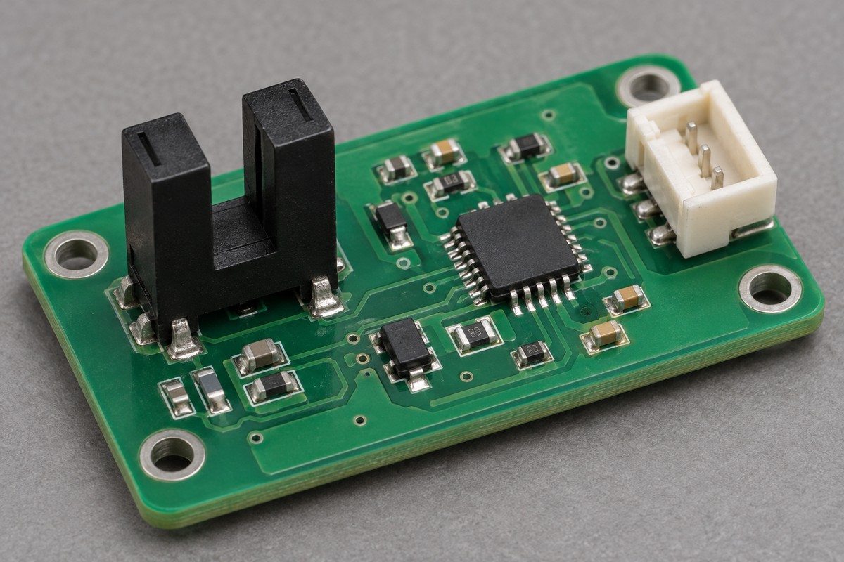
Optical sensor PCB assembly includes mounting and soldering the sensing devices, their supporting electronics, and the board’s connectors, followed by inspection and the specified tests. The optical arrangement determines which assembly details matter most.
| Sensor arrangement | How it detects | Assembly detail that affects operation |
|---|---|---|
| Reflective sensor | A receiver detects light returned from a target | Emitter and receiver orientation, spacing, and clearance toward the target |
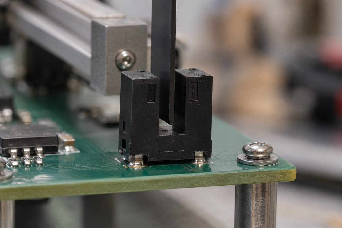
| Transmissive or slotted sensor | An object interrupts a beam between an emitter and receiver | Slot position relative to the moving flag, strip, or disc |
| Ambient light or color sensor | A detector measures incoming light | An unobstructed opening and the intended filter or cover |
| Time-of-Flight sensor | A module measures distance using emitted and returned light | Module orientation and compatibility with the cover-window arrangement |
Some devices integrate the emitter and receiver into one package; an ambient light detector does not require its own emitter. An optical encoder PCB, for example, must place its sensing elements correctly relative to the patterned disc or strip that provides position feedback.
The populated board and any separately mounted optical or mechanical parts form one sensing arrangement. Their assembly relationship deserves the same attention as the solder joints.
How Do Sensor Height and Tilt Affect the Optical Path?
Height and tilt change where the sensor looks and whether its light path clears surrounding parts. Correct pad placement alone does not guarantee correct alignment after soldering and installation.
- Sensor height sets the relationship between the optical face and the target, slot, or enclosure opening. A leaded device mounted above its intended seating position can shift that relationship.
- Sensor tilt changes the viewing direction. As a simple geometric example, a 1° angular change shifts the optical axis by about 1.75 mm at a distance of 100 mm. This illustrates geometry, not a recommended assembly tolerance.
- Board mounting position determines alignment with features outside the PCB. A correctly soldered sensor can still be offset from a housing aperture if the board is seated incorrectly.
For leaded sensors, locating features or fixtures can hold the intended position while joints are formed. Leads should be shaped before soldering according to the package instructions, rather than forced into alignment afterward. The assembly drawing should relate the optical face to a usable reference, such as a mounting hole or enclosure feature, so inspection addresses the installed position.
How Are Optical Sensors Protected During Soldering?
The soldering process must form reliable joints within the optical component’s permitted thermal and handling limits. A profile suitable for the other ICs on the board may not suit its sensor package.
Three controls are especially relevant to production.
- Moisture exposure. Moisture-sensitive packages need storage and floor-life control based on their specified moisture sensitivity level. Baking, when required, must follow the device and packaging instructions.
- Temperature over time. Peak temperature, heating rate, and exposure duration all matter. The profile is verified on the assembled board, including the sensor location, rather than assumed from the oven setting.
- Subsequent heating. A second soldering operation or local repair adds thermal exposure. Its compatibility must be considered before the board enters production.
For through-hole devices, lead soldering must also avoid transferring excessive heat or mechanical stress into the body. There is no single reflow temperature, baking schedule, or permitted number of soldering cycles for all optical sensors. Those limits belong to the exact part being assembled.
How Can Assembly Keep Sensor Windows Free of Contamination?
Keeping contamination away from the optical surface is preferable to relying on cleaning after assembly. A cleaning process that works for exposed solder joints can damage a sensor’s resin, coating, or optical package.
Handling can be organized around the surface that needs protection.
- Keep fingers and tools away from optical faces; grip the board at suitable edges or handling areas.
- Use the component manufacturer’s permitted pickup and protection methods. A protective film is retained or removed at the specified process stage, not automatically left through soldering.
- Control soldering residues and debris from nearby operations so they do not reach the sensor opening.
- Inspect the optical surface before functional testing and protect it during subsequent handling and packing.
“No-clean” flux does not mean residue is harmless on an optical window. Electrical residue acceptability and optical cleanliness are different requirements. Likewise, solvent cleaning or ultrasonic washing is not a universal remedy. The VL53L1X, for example, has device-specific no-wash handling guidance; that instruction must not be generalized into a cleaning recipe for other packages.
If contamination is found, the recovery method depends on the component’s approved cleaning instructions. Unvalidated wiping can replace a removable particle with a scratched or smeared surface.
Why Can a Cover Window Change the Sensor Reading?
A cover window becomes part of the optical path. Its material and geometry can change the light reaching the detector even when the electronics remain unchanged.
For a covered ToF module, three effects deserve particular attention.
| Window feature | Possible effect on sensing |
|---|---|
| Material or coating transmission | Less useful light passes at the sensor’s operating wavelength |
| Reflections within the window | Some emitted light reaches the receiver without following the intended target path, creating optical crosstalk |
| Aperture, air gap, or window tilt | The emitter or receiver cone may be restricted or interact differently with the cover |
A window that appears dark to the eye may transmit infrared, while visual transparency alone does not prove suitability at the operating wavelength. In suitable ToF designs, a correctly fitted optical barrier between transmit and receive paths helps limit unwanted coupling without blocking the useful light cones.
Changing the window, coating, or gasket therefore calls for an optical performance review. Testing an uncovered board cannot, by itself, establish its performance behind the final cover.
How Are Optical Sensor Boards Functionally Tested?
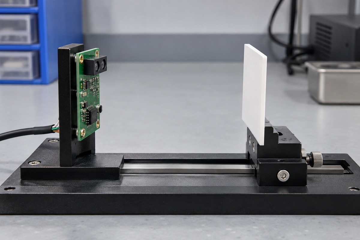
Functional testing applies a defined optical stimulus and measures the board’s response. Power and communication checks establish that the electronics operate; the optical test addresses whether the assembled board detects what it should.
| Board function | Example test stimulus | Response to measure |
|---|---|---|
| Object detection | A defined target placed inside and outside the intended detection region | Detection output in both states |
| Slotted sensing | A specified flag moved through and clear of the slot | Output transitions and repeatability |
| Distance measurement | A target at defined reference positions | Reported distance and valid-reading status |
| Ambient light measurement | Controlled illumination at specified levels | Output across those levels |
These are test-plan examples, not universal pass limits. Target position, relevant surface properties, ambient illumination, supply conditions, and software settings need to be controlled sufficiently for results from different boards to be comparable.
For example, moving a hand in front of a reflective sensor shows that it reacts. It does not provide a repeatable acceptance test because hand position and reflected light vary. A fixture with a defined target makes a failed result easier to distinguish from a changed test setup.
AOI can identify visible assembly defects, but it does not measure sensing performance. Production testing uses the applicable limits established for the design; broader operating-range validation determines whether those limits adequately represent the product’s intended use.
When Is Calibration Needed After Sensor Assembly?
Calibration is needed when the selected sensor or product design requires correction for device variation or the installed optical arrangement. Some threshold-based boards only need functional verification; others require calibration during manufacturing.
The VL53L1X illustrates why the sequence matters. Its manufacturing flow includes offset calibration to compensate for effects including reflow and cover glass. Additional calibration steps apply when a protective cover glass is added. These are requirements of that device and its integration, not a rule for every optical sensor board.
Calibration and verification serve different purposes.
- Calibration derives correction values using the prescribed reference conditions.
- Verification measures performance after those values are applied, against the required acceptance limits.
- Restart testing, where applicable, confirms that the stored correction values are loaded and used again.
Calibration should occur in the assembly state required by the device procedure. A later change to the sensor or optical stack may invalidate its correction values and require recalibration. A blocked aperture, displaced component, or contaminated window is an assembly problem to resolve before treating the reading as a calibration error.
FAQs About Optical Sensor PCB Assembly
Does optical sensor PCB assembly always require a cleanroom?
No. The required environment depends on the exposed optical surfaces, contamination limits, and product specification. Assembly of packaged sensors does not automatically carry the same cleanliness requirements as exposed image-sensor or lens-module assembly.
When is X-ray inspection useful for an optical sensor board?
It is useful when the selected packages have hidden solder joints that need examination. X-ray inspection addresses the joints; it does not establish window cleanliness, optical alignment, or detection accuracy.
Can conformal coating cover the sensor window?
Only if that optical coating arrangement is explicitly supported and validated. Otherwise, the sensing surface and necessary light-path clearances remain coating keep-out areas. A material that looks clear can still alter optical performance.
Does a sensor board need another functional test after rework?
Yes, the affected functions should be retested. Rework can alter the sensor’s position, expose it to additional heat, or contaminate nearby optics. Recalibration may also be necessary if the device procedure or changed assembly requires it.
Why can an uncovered board pass while the finished product fails?
The finished product adds the housing, window, mounting position, and sometimes optical barriers. These can obstruct or redirect light. Board-level testing and finished-assembly testing therefore need conditions appropriate to the assembly state they are evaluating.
Consistent optical sensor PCB assembly depends on preserving the intended optical path through soldering, handling, and final integration. EBest Circuit can support fabrication and assembly to your approved design, with inspection and functional testing agreed for the build. Discuss your board’s sensor package, assembly requirements, and test needs with sales@bestpcbs.com.