





An optocoupler pinout identifies the input LED terminals and the output connections, but the pin numbers depend on the exact device. A PC817 has four pins, a 4N35 adds an accessible transistor base, and a 6N137 needs a powered output circuit. Finding the correct pin map first prevents reversed connections and helps you choose the right wiring arrangement.
EBest Circuit (Best Technology) supports PCB fabrication, component sourcing, and PCB assembly for boards using optocouplers. DFM review and assembly inspection help address footprint fit, component orientation, and soldering before boards reach functional testing. For support with your PCB or PCBA project, contact sales@bestpcbs.com.
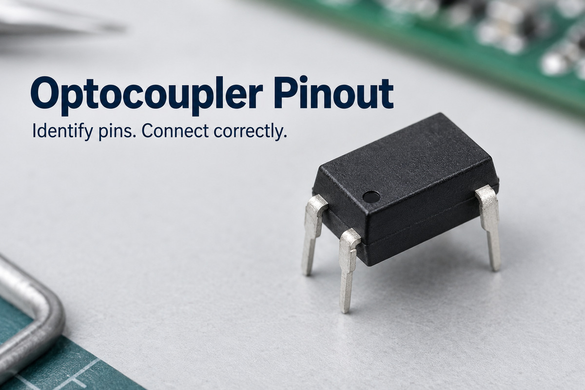
PC817 Optocoupler Pinout
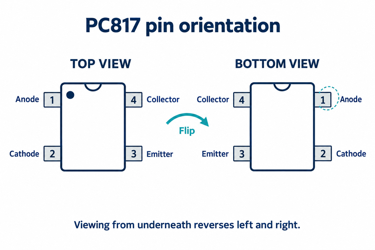
The PC817 uses pins 1 and 2 for its input LED, and pins 3 and 4 for its output phototransistor.
| Pin | Terminal | Function |
|---|---|---|
| 1 | Anode | LED input; receives forward current through a limiting resistor |
| 2 | Cathode | LED return |
| 3 | Emitter | Phototransistor return in a typical switching circuit |
| 4 | Collector | Output node in a typical pull-up circuit |
The LED transfers the signal optically to the transistor. There is no internal conductive connection between the input pair and the output pair.
Pin 4 is the collector, not the emitter. Swapping these terminals can produce misleading behavior rather than a reliable switch. Use the package drawing for the exact manufacturer and suffix when matching these numbers to physical leads.
4N35 Optocoupler Pinout
The 4N35 has six pins, including one NC pin and a separate transistor base connection.
| Pin | Terminal | Function |
|---|---|---|
| 1 | Anode | Input LED anode |
| 2 | Cathode | Input LED cathode |
| 3 | NC | No internal connection |
| 4 | Emitter | Output transistor emitter |
| 5 | Collector | Output transistor collector |
| 6 | Base | Access to the output transistor base |
In a basic phototransistor switching circuit, the base can be left open. Some circuits add a base-emitter resistor to alter sensitivity and switching behavior; it is not a mandatory connection for every application.
Pins 3 and 6 serve different purposes. Pin 3 is unused internally, while pin 6 connects to the transistor. Grounding the base simply because it looks like an unused terminal can change how the device operates.
How Does the 6N137 Pinout Differ from the PC817?
The 6N137 has a powered logic output, so its extra pins include VCC, ground, and enable. It cannot use the PC817 wiring arrangement unchanged.
| Pin | Terminal | Function |
|---|---|---|
| 1 | NC | No connection |
| 2 | Anode | Input LED anode |
| 3 | Cathode | Input LED cathode |
| 4 | NC | No connection |
| 5 | GND | Output-side ground |
| 6 | VO | Signal output; requires a pull-up |
| 7 | VE | Output enable control |
| 8 | VCC | Output-side supply |
For the Vishay 6N137, the recommended supply range is 4.5–5.5 V. A 0.1 µF bypass capacitor belongs close to pins 8 and 5. With enable high, LED current turns the output low; pulling enable low disables that response and lets the pull-up hold the output high.
Pin 5 is the output circuit's reference. It does not need to connect to the LED-side return for the signal to cross the isolation barrier.
How Do You Identify Pin 1 on an Optocoupler?
Locate the manufacturer's pin-1 mark, then read the package drawing from its stated viewing direction. Printed text orientation alone is not a reliable pin-number reference.
- Find the orientation mark. Depending on the package, this may be a dot, notch, or another feature identified in the mechanical drawing. A molding mark is not automatically a pin-1 indicator.
- Establish the viewing side. A top view looks down onto the component body. A bottom view looks toward the leads from underneath and reverses the apparent left-right arrangement.
- Follow the numbering around the package. For a conventional DIP viewed from above with its notch at the top, pin 1 is at the upper left. Numbers run down the left side and return up the right side.
For example, a six-pin DIP in that orientation has 1–2–3 down the left and 6–5–4 down the right. This places the 4N35 collector, pin 5, midway down the right side.
On a PCB, pad 1 must agree with the schematic pin number and assembly orientation. A correct circuit symbol still produces a wrong board if its footprint numbers are mirrored.
How Do You Wire a PC817 Optocoupler?
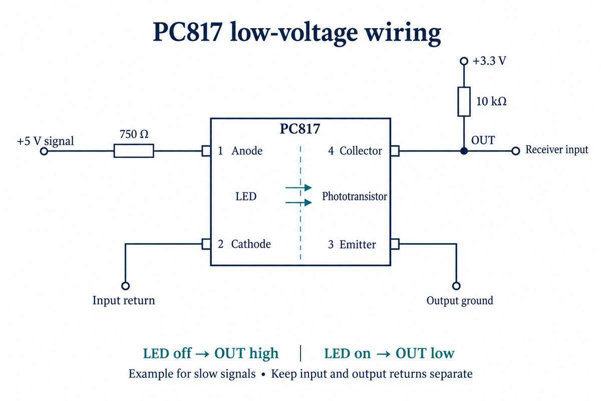
A simple PC817 interface uses a series resistor on the LED side and a pull-up resistor on the collector side. The example below is for a low-voltage, slow switching signal, such as an on/off status input.
Input-side connections
- Connect the 5 V input signal through a 750 Ω resistor to pin 1.
- Connect pin 2 to the input-side return.
- Use a signal source that can supply approximately 5 mA.
Using an assumed LED forward drop of 1.2 V, the estimated input current is (5 − 1.2) / 750 ≈ 5.1 mA. This is an example calculation; actual current also depends on the source voltage and the LED's forward voltage.
Output-side connections
- Connect pin 3 to the receiving circuit's ground.
- Connect pin 4 through a 10 kΩ pull-up resistor to the receiving circuit's 3.3 V supply.
- Connect the receiving input to pin 4.
The pull-up requires approximately 0.33 mA when the output is near ground, excluding other load current. These values provide a light load for a bench demonstration. A production design must also meet the receiving input's voltage thresholds across component variation and temperature.
The output is inverted. With the LED off, the pull-up holds pin 4 high. With adequate LED current, the transistor pulls pin 4 low. The transistor sinks current; it does not generate the output-side supply voltage.
To retain galvanic isolation, keep the two returns separate and power the sides from appropriately isolated sources. A shared supply return or an instrument ground connection can join them externally.
How Do You Test a PC817 Optocoupler?
Test the input LED first, then verify that input current changes the output voltage. A diode reading alone cannot prove that the complete optocoupler works.
1. Check the input LED with power removed
For a loose device, use the meter's diode mode with the red probe on pin 1 and the black probe on pin 2. A working input normally shows a forward diode reading; reversing the probes normally shows an open indication. The displayed voltage depends on the meter's test current.
A near-zero reading in both directions suggests a short. An open indication both ways may mean an open LED, incorrect contact, or an unsuitable meter test range. In-circuit measurements can be affected by surrounding components.
2. Check optical switching with a low-voltage supply
Use the example circuit above. Keep the 3.3 V output supply connected and measure pin 4 relative to pin 3. Switch the LED input off and on.
| Observation | Likely explanation or next measurement |
|---|---|
| Output changes from near 3.3 V to a low voltage | The device transfers an on/off signal in this test circuit |
| Output stays high | Measure the voltage across the 750 Ω resistor to establish whether LED current flows; also check collector/emitter orientation |
| Output stays low with the LED off | Look for an output short, incorrect wiring, or another circuit pulling the node low |
Input current can be calculated from the measured resistor voltage using I = V / 750 Ω. This avoids guessing whether the LED is receiving current.
Passing this test does not establish switching speed, guaranteed CTR, or insulation performance. Those need measurements appropriate to the actual application.
Are Optocouplers with the Same Pinout Interchangeable?
Matching pin numbers is necessary for a direct replacement, but it does not establish electrical or mechanical compatibility. A substitute can fit the board and still change the output signal.
- CTR and drive current. In a phototransistor optocoupler, a lower current transfer ratio can leave too little collector current to pull the output low. Compare guaranteed values at relevant LED current and temperature, not just typical values.
- Switching behavior. A device that passes a static on/off test may distort short pulses. Load resistance and transistor saturation also affect the waveform.
- Operating limits. Collector voltage, LED reverse voltage, current, and temperature ratings must suit the circuit. Absolute maximum ratings are not recommended operating points.
- Package and isolation geometry. Lead pitch, lead form, body dimensions, and insulation specifications can differ even when the terminal names match. The PCB's spacing must remain suitable as well.
Output type is another distinction that a similar-looking package can hide. A phototransistor, a powered logic-output device, and a TRIAC-output optocoupler do different jobs.
When approving alternative electronic components for an existing assembly, retain the full manufacturer part number and validate the substitute in the actual circuit. A matching footprint alone is not enough to call it a drop-in replacement.
FAQs About Optocoupler Pinout
Can an NC pin be used as a convenient PCB connection point?
Leave it unconnected unless the exact device documentation permits another use. An NC label is not an invitation to route unrelated signals through that pad; doing so may also affect spacing around the isolation barrier.
Do both sides of an optocoupler need a common ground?
No. Optical signal transfer works with separate input and output references. Connecting their grounds creates an external conductive path and removes galvanic separation between those references.
What happens if the input LED is connected backward?
It will not produce the intended optical signal. Excessive reverse voltage can damage it, so reverse connection is not a valid way to turn the device off.
Do optocoupler suffixes change the pinout?
Not necessarily. A suffix may identify a CTR grade, lead form, packaging option, or approval option. Its meaning is manufacturer-specific; the complete order code determines which package drawing and specifications apply.
Is an optocoupler module's terminal layout the same as the bare device's pinout?
Usually it is different. Modules can add resistors, indicators, connectors, and other circuitry. Follow the module's terminal labels and schematic rather than assigning chip pin numbers to its screw terminals.
Getting the optocoupler pinout right is the starting point for consistent board assembly. EBest Circuit supports PCB fabrication, sourcing, and PCBA for your approved circuit and component requirements. Discuss your next build with sales@bestpcbs.com.
You may also like





Tags: Optocoupler Pinout, Optocoupler Wiring, PC817 Optocoupler