





The name sounds simple, but the engineering is not. A weak interface can corrupt data, expose a processor to surge energy, create ground loops, or turn a serviceable module into a difficult assembly. This guide explains how interface boards work and what engineers should verify before releasing one for PCB fabrication and assembly.
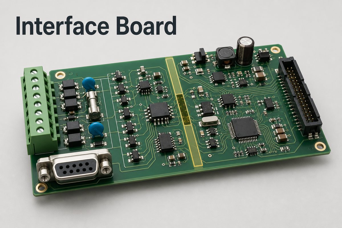
What Is an Interface Board?
An interface board is a printed circuit board placed between two functional blocks to make their electrical, communication, or mechanical connection usable. One side may face a sensor, actuator, display, cable, test fixture, or field device. The other side may connect to a microcontroller, FPGA, computer, power stage, or larger control system.
The practical interface board meaning depends on the system. In one machine, it is a simple connector adapter. In another, it is an active interface circuit board containing transceivers, isolation, filtering, protection, and local diagnostics. The phrase circuit board interface can also refer to the complete electrical and mechanical boundary between that PCB and the connected equipment. The defining feature is its boundary role: it manages what crosses from one subsystem to another.
An interface board is not automatically a complete controller. It may contain a processor, but its main responsibility is still to manage the interface rather than execute the system’s primary control algorithm.
What Does an Interface Board Do?
A good interface board converts an uncertain external connection into a controlled electrical environment. Its exact functions depend on the source, destination, cable length, protocol, voltage, bandwidth, and fault exposure.
- Signal adaptation: translates voltage levels, logic families, single-ended signals, or differential standards.
- Protocol support: implements physical-layer interfaces such as RS-232, RS-485, CAN, USB, Ethernet, I2C, SPI, or LVDS.
- Analog conditioning: filters, amplifies, biases, linearizes, or converts sensor signals before an ADC.
- Protection: limits ESD, surge, reverse polarity, overvoltage, overcurrent, and cable-discharge stress.
- Isolation: separates ground domains to improve safety, noise immunity, or system robustness.
- Power interfacing: regulates, switches, sequences, or monitors power delivered across the boundary.
- Mechanical adaptation: converts one connector, pinout, cable orientation, or board position to another.
- Service access: provides indicators, test points, programming headers, loopback paths, or replaceable modules.
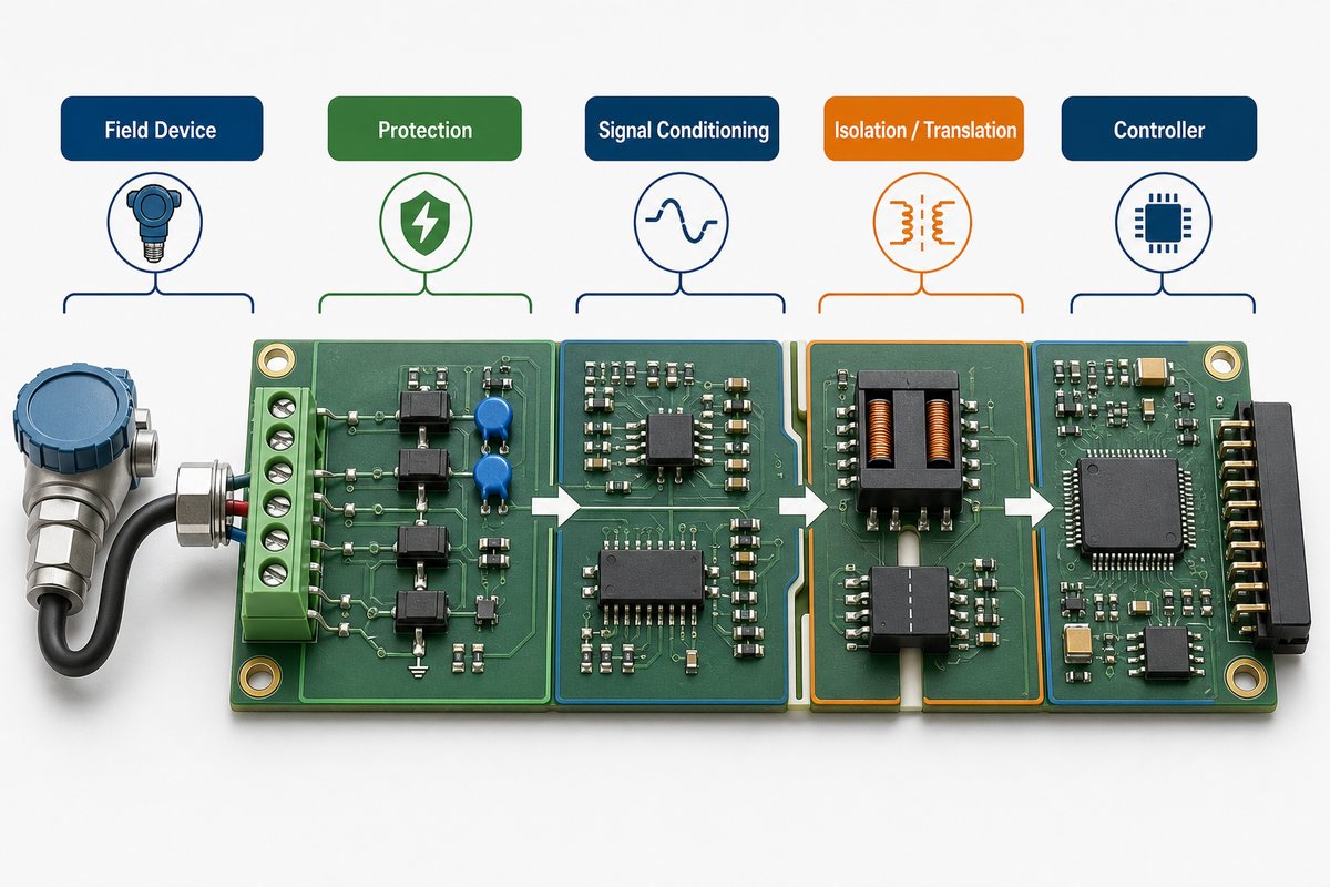
These functions often appear together. For example, an industrial sensor input may need surge protection, a filter, galvanic isolation, level translation, and a diagnostic LED before the signal reaches the controller.
How Is an Interface Board Different From a Controller or Main Board?
The distinction is based on system responsibility, not board size. An interface board manages a boundary. A controller board makes control decisions. A main board integrates the central processing, memory, power, and primary peripherals of the product.
| Board | Primary Role | Typical Circuits |
|---|---|---|
| Interface board | Connects and protects two subsystems | Transceivers, filters, isolation, level shifters, connectors |
| Controller board | Reads inputs and executes control logic | MCU or FPGA, memory, timing, I/O, control firmware |
| Main board | Hosts the product’s central electronics | Processor, memory, power tree, buses, major peripherals |
| Passive adapter board | Changes connector or pinout only | Connectors, traces, optional jumpers or test points |
One PCB can serve more than one role. An interface control board may contain both the physical interface and local control logic. The design files should make that division clear so reviewers know which circuits face external faults and which circuits belong to the protected logic domain.
Which Interface Board Types Are Common?
Interface boards are usually classified by what they connect or by the physical layer they implement.
| Type | Main Function | Design Focus |
|---|---|---|
| Serial interface board | Connects UART, RS-232, RS-422, or RS-485 equipment | Termination, biasing, common-mode range, isolation |
| CAN interface board | Connects controllers or nodes to a CAN bus | Transceiver placement, 120-ohm termination, ESD and surge |
| User interface board | Supports displays, LEDs, switches, encoders, or touch inputs | Mechanical alignment, visible indicators, cable durability |
| Sensor interface board | Conditions low-level analog or digital sensor outputs | Noise, offset, gain, filtering, reference integrity |
| Power interface board | Distributes or switches power between modules | Current capacity, heat, protection, creepage and clearance |
| ATE device interface board | Connects automatic test equipment to a device under test | Pin mapping, signal fidelity, fixture wear, replaceability |
| Universal interface board | Supports several configurations through jumpers or modules | Configuration control, labeling, unused-node behavior |
Some products divide these functions across modules. That approach can simplify service and upgrades, but every board-to-board connection adds pinout, stack height, return-path, tolerance, and supply-chain considerations. A disciplined modular PCB design process is useful when the interface is intended to be replaceable.
What Belongs in an Interface Board PCB?
An interface board PCB should contain only the circuits needed to make the boundary safe, measurable, and reliable. Adding unnecessary processing makes fault analysis harder; omitting protection shifts risk into a more expensive controller.
Common functional blocks include:
- input and output connectors with unambiguous pin 1 and polarity markings;
- TVS diodes, fuses, resettable protection, current limiting, or reverse-polarity protection;
- common-mode chokes, ferrites, RC filters, termination networks, and bias resistors;
- transceivers, level shifters, isolators, ADCs, DACs, or instrumentation amplifiers;
- local regulators, sequencing, decoupling, and power-good monitoring;
- status indicators, test points, programming access, and board identification;
- mounting holes, keepouts, shields, cable retention, and enclosure interfaces.
The schematic should define the operating state of every line during power-up, reset, unplugging, and partial power. Interfaces fail surprisingly often because one side is powered while the other is not.
How Should a PCB Interface Handle Signals and Power?
A PCB interface must be designed from the electrical limits inward. Start with the source and load voltage ranges, thresholds, current, edge rate, common-mode range, cable impedance, and maximum expected fault. Do not select a translator or transceiver from protocol name alone.
For digital links, check:
- logic-high and logic-low margins across temperature and supply tolerance;
- whether either side can be unpowered while signals remain present;
- direction control and fail-safe behavior for bidirectional devices;
- termination placement and topology for differential or multidrop buses;
- edge rate rather than clock frequency when deciding whether routing behaves as a transmission line;
- return-path continuity through connectors and across reference-plane changes.
Fast USB, Ethernet, LVDS, memory, and display links need the same impedance, return-path, and crosstalk discipline described in high-speed PCB design. A slow data rate does not guarantee a forgiving layout if the driver edge is fast.
For analog channels, define source impedance, bandwidth, acceptable noise, gain error, offset, input bias, anti-alias filtering, and ADC reference strategy. Keep high-current switching loops away from high-impedance sensor nodes.
Power paths require a separate budget for startup current, steady-state current, transient load, connector derating, copper temperature rise, regulator loss, and fault energy. If the board passes power through to another module, provide enough test access to measure drop under load.
How Should Protection, Isolation, and Grounding Be Designed?
Protection components work only when their current path is intentional. A TVS diode placed far from the connector can allow the ESD current to travel through sensitive circuitry before it reaches the clamp.
- Place the first protection stage close to the exposed connector.
- Use short, wide paths from the protection device to its intended return.
- Keep the protected side physically distinct from the field side.
- Do not route sensitive traces through a surge-current loop.
- Confirm the clamping voltage is safe for the downstream IC, not merely that a TVS is present.
- Coordinate fuses, current limiters, MOSFETs, and transient suppressors so one device does not defeat another.
Galvanic isolation is useful when grounds can differ, noise is severe, or a safety boundary is required. It also adds isolated power, propagation delay, creepage, clearance, and component qualification requirements. Split grounds should not be used as a decorative layout technique; they require a clear current-flow reason.
In an industrial interface board, shielding and chassis connection deserve early attention. Decide where cable shields terminate and whether the connection is direct, capacitive, or application-dependent. Leaving that decision until layout review often creates an awkward current path.
Which Connector and Mechanical Details Matter?
Connectors define more failures than their schematic symbol suggests. Confirm the mating part, pin numbering, keying, insertion cycles, contact current, voltage rating, retention, vibration exposure, cable bend radius, and assembly access.
Useful design checks include:
- keep pin 1, polarity, port name, and cable direction visible after assembly;
- leave enough room for latch release and technician fingers;
- keep tall connectors away from enclosure ribs and fasteners;
- add mounting support where cable force could flex the PCB;
- define plated and non-plated holes correctly in the fabrication data;
- check board-edge tolerances for card-edge, press-fit, or panel-mounted interfaces;
- avoid test points under installed cables or inaccessible shields.
When USB is part of the design, connector generation and cable orientation affect both layout and user handling. Our overview of USB interfaces from Type-A to Type-C provides additional connector context.
How Should an Interface Board Be Laid Out?
Layout should follow the direction of energy and information: connector, protection, filtering, translation or isolation, then protected logic. That sequence makes the board easier to review and prevents traces from crossing back into the unprotected region.
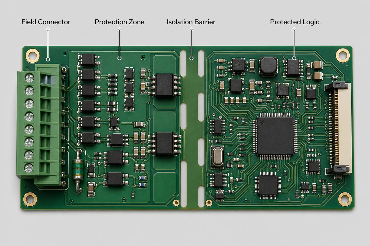
During placement and routing, verify:
- decoupling capacitors have short connections to the power and ground pins they serve;
- differential pairs maintain geometry, spacing, symmetry, and a continuous reference plane;
- isolation barriers have no copper, test point, mounting hardware, or silkscreen feature that violates the required spacing;
- high-current loops are compact and separated from analog inputs;
- connector shields and chassis returns do not inject noise into digital ground;
- series resistors, terminators, filters, and clamps are placed where their electrical function requires them;
- test points do not create long stubs on high-speed nets.
A four-layer board with solid references is often easier to control than a crowded two-layer board, but layer count should follow routing density, signal integrity, isolation, current, and EMC needs. The lowest layer count is not always the lowest system cost if it increases debug or compliance risk.
How Are Interface Boards Manufactured and Assembled?
Interface boards frequently mix fine-pitch ICs with large connectors, terminal blocks, relays, shields, or through-hole parts. That component mix affects panelization, stencil design, reflow, selective soldering, hand-solder limits, fixture clearance, and inspection access.
A manufacturing review should confirm:
- the stackup and controlled-impedance requirements match the routed geometry;
- copper weight supports the current and thermal targets;
- annular rings and hole sizes suit the selected connector pins and tolerances;
- component-to-edge spacing supports depaneling and connector overhang;
- large thermal masses will not create soldering imbalance or insufficient hole fill;
- polarity, reference designators, and port labels remain readable;
- the assembly drawing identifies fitted, optional, and configuration-dependent parts.
If the interface is part of a larger machine controller, coordinate its fabrication and assembly assumptions with the main industrial control PCB. Misaligned connector pinouts and different ground assumptions are system problems, even when both boards pass standalone inspection.
How Should an Interface Board Be Tested?
Bare-board electrical test confirms continuity and isolation of the PCB, but it cannot prove that an assembled interface performs correctly. The test plan should follow the board’s boundary functions.
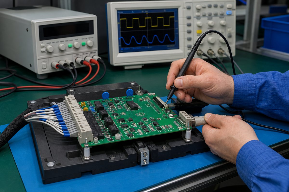
A practical test sequence may include:
- Unpowered checks: shorts, resistance, polarity, connector mapping, and isolation resistance.
- Controlled power-up: current-limited supply, rail sequencing, regulator outputs, and abnormal heating.
- Static I/O checks: thresholds, pull states, indicators, enables, and fault outputs.
- Dynamic signal checks: amplitude, timing, rise/fall behavior, eye quality, bus errors, and termination.
- Fault checks: open cable, reversed supply, shorted load, missing termination, or powered/unpowered side combinations where safe and specified.
- Functional test: known-good host and field-side emulators, or a dedicated fixture that exercises every supported channel.
For an ATE device interface board design, fixture contact life and replaceable wear parts matter as much as first-pass electrical performance. Define calibration, golden-unit control, retest rules, and test-log traceability before volume production.
Where Is a Hardware Interface Board Used?
A hardware interface board is useful wherever a product needs a controlled boundary between electronics, cables, users, field wiring, or test equipment. Common applications include:
- industrial automation, PLC I/O, motor drives, and machine controllers;
- medical and laboratory instruments with isolated sensors or replaceable probes;
- energy systems, battery equipment, chargers, and monitoring units;
- transportation electronics and distributed CAN or LIN nodes;
- display panels, keypads, control consoles, and human-machine interfaces;
- telecommunications, networking, and high-speed data modules;
- production test fixtures, programming stations, and device characterization systems.
The board may be small, but its position at the system edge makes reliability important. External cables, operators, service tools, and field devices bring uncertainty that protected logic never sees directly.
FAQ About Interface Boards
Is an interface board always an active PCB?
No. A passive board may only adapt a connector or pinout. An active board adds protection, buffering, translation, isolation, filtering, conversion, power control, or diagnostics.
Can an interface board contain a microcontroller?
Yes. A microcontroller may handle protocol conversion, identification, diagnostics, timing, calibration, or local I/O. The board remains an interface board if its primary system role is managing the boundary.
When is isolation needed?
Isolation is considered when ground potential can differ, common-mode noise is high, safety requires separation, or a field-side fault must not reach protected logic. The required voltage and creepage depend on the actual application and standard.
Can a two-layer PCB be used?
Yes for simple, low-density, low-speed circuits when current, EMC, and return paths remain controlled. Four or more layers are often preferable when the board combines fast signals, sensitive analog channels, isolation, or dense connectors.
What files are needed for manufacturing?
Provide Gerber or ODB++ fabrication data, drill files, stackup and impedance requirements, BOM, centroid data, assembly drawings, schematics where available, test requirements, and notes for optional configurations or programmed devices.
How Can EBest Circuit Support Your Interface Board Project?
At EBest Circuit, we have provided PCB and PCBA services since 2006. We support prototypes and production with PCB fabrication, component sourcing, assembly, and engineering review. Our documented quality and compliance references include ISO 9001:2015, ISO 13485:2016, IATF 16949, AS9100D, RoHS, REACH, and UL information, subject to the applicable product and project scope.
For interface projects, we can review stackup, controlled-impedance requirements, connector footprints, isolation spacing, manufacturability, assembly access, and the test information needed for the build. Our inspection and test resources include AOI, X-ray inspection, electrical test, flying-probe test, impedance testing, micro-section inspection, and functional testing as applicable.
Send your Gerber files, BOM, stackup, quantity, assembly requirements, and test plan to sales@bestpcbs.com. Tell us what the interface board connects, the voltage and protocol on each side, and any isolation, EMC, mechanical, or environmental constraints. We will review the manufacturing package and help identify questions before production.
You may also like





Tags: circuit board interface, hardware interface board, Interface Board, interface board pcb, pcb interface