





A reliable signal transmission PCB begins with one coordinated channel definition: driver edge rate, target impedance, stackup, trace geometry, return path, connectors, vias, termination, and acceptance testing. If any of these inputs changes after routing, the manufactured board may no longer match the simulation or interface requirement.
Identify interconnects whose electrical length, loss, coupling, or discontinuities can alter the received waveform. These paths need controlled geometry, documented fabrication assumptions, and verification from prototype through production.
What Is a Signal Transmission PCB?
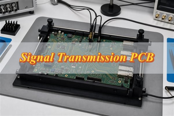
A signal transmission PCB controls waveform quality. The design must keep reflection, attenuation, skew, crosstalk, and EMI within the receiver’s margin. Traces, reference planes, vias, connectors, and termination therefore form one electrical structure.
The board may carry digital links, clocks, memory buses, video, Ethernet, USB, LVDS, RF, or precision analog signals. Risk depends on edge rate, channel length, loss budget, receiver margin, and return-path geometry. A low clock frequency can still cause transmission-line behavior when its driver edge is fast.
Check these three structures before classifying a route as controlled:
- Signal conductor: Define the routing layer, finished width, copper thickness, pair spacing, maximum skew, and every pad or via transition.
- Dielectric system: Define the pressed dielectric thickness, design Dk and Df, glass construction, copper profile, and allowed material equivalents.
- Return path: Name the reference layer, prohibit split or void crossings, and provide a return transition beside each signal-layer change.
Minimum release evidence: The fabrication package should contain a controlled-net table, approved stackup, impedance targets and tolerances, coupon requirements, and the required test-report format. Without these items, the supplier cannot verify that the manufactured structure matches the intended channel.
When Does a PCB Trace Behave as a Transmission Line?
Compare signal edge time with interconnect propagation delay. A trace needs transmission-line treatment when the signal can change substantially before the wave has propagated through the interconnect and returned. Use the driver’s fastest rise or fall time, not the protocol clock alone.
Calculate the boundary in five steps:
- Find the fastest edge. Use the maximum slew-rate condition from the datasheet, IBIS model, or measured source waveform. Include faster replacement parts if substitutions are allowed.
- Build the full electrical length. Include package escape, PCB trace, vias, connector, cable, branches, and receiver escape. Do not evaluate only the straight routed segment.
- Calculate one-way delay. Multiply each segment length by its modeled delay per unit length. Use the correct effective dielectric behavior for outer-layer and inner-layer structures.
- Compare delay with edge time. If the ratio is not clearly small, model the interconnect as a transmission line. Avoid a universal inch or frequency threshold because stackup and edge rate change the result.
- Apply the receiver limit. Check overshoot, undershoot, settling, jitter, eye opening, and input-protection limits. The receiver requirement determines whether the predicted discontinuity is acceptable.
Escalate uncertain routes to simulation. Use the production stackup, driver and receiver models, connector model, termination, and via geometry. The high-speed PCB design guide provides additional routing and stackup context. Record the model revision and acceptance limit so the result can support design release.
How Do Microstrip, Stripline and Coplanar Waveguide Structures Differ?
The structures differ mainly in field containment. Microstrip is an outer-layer trace, while stripline is embedded between reference planes. Coplanar waveguide adds grounded copper beside the signal on the same layer. The correct choice depends on routing access, loss, density, launch geometry, and fabrication tolerance.
| Comparison dimension | Microstrip | Stripline | Coplanar waveguide with ground |
| Trace location | Outer layer over one main reference plane | Inner layer between reference planes | Usually outer layer with side grounds and a lower reference plane |
| Field exposure | Partly in air and partly in dielectric | Mostly contained within dielectric | Shared among side grounds, lower plane, air, and dielectric |
| EMI and shielding | More exposed to nearby structures | Better field containment when planes remain continuous | Good lateral field control when gaps and ground-via spacing are consistent |
| Inspection and probing | Easy physical access | Buried and not directly probeable | Accessible, but side-ground geometry constrains probe and component placement |
| Manufacturing sensitivity | Etch, plating, solder mask, and dielectric height | Etch, core/prepreg thickness, resin flow, and layer registration | Trace width, copper thickness, side gap, mask condition, and via-fence geometry |
| Typical use | Short high-speed routes, accessible launches, antennas, and general controlled impedance | Dense digital channels needing isolation and predictable reference planes | RF launches and routes needing compact grounding or stronger field confinement |
| Main limitation | Greater exposure and possible radiation or coupling | More vias may be needed to reach components, adding discontinuities | Small side gaps can be difficult to hold and may limit routing density |
Selection rule: Use microstrip when access and a short launch matter; use stripline when isolation and field containment matter; use grounded coplanar waveguide when lateral grounding supports the launch. In every case, recalculate finished impedance with the actual mask, plating, etched shape, adjacent copper, and dielectric construction.
How Should Materials and Stackups Be Selected for Signal Transmission PCBs?
Start with the loss budget and a producible stackup. Signal transmission PCB material selection must account for impedance, routing density, frequency, temperature, and available constructions. Standard FR-4 suits many digital channels, but no universal frequency or data-rate limit makes every FR-4 construction acceptable.
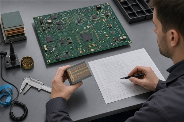
Use these five decisions to release the stackup:
- Set the channel limits. Define allowable insertion loss, return loss, delay, skew, temperature, voltage, and reliability.
- Assign every reference plane. Keep critical signal layers beside solid references and minimize plane changes.
- Use frequency-relevant material data. Confirm Dk, Df, test method, frequency, resin content, and glass style with the supplier.
- Check manufacturable geometry. Balance trace width and dielectric thickness against routing density, loss, and etch tolerance.
- Freeze the production stackup. Approve substitutions and require impedance recalculation before any material or construction change.
Choose the material by channel margin, not by data rate alone:
| Check | Standard FR-4 is suitable when | Consider low-loss or hybrid when | Confirm before release |
| Channel loss | The modeled channel retains enough margin | FR-4 loss consumes the available margin | Channel length, spectrum, and insertion-loss limit |
| Dielectric data | Available Dk and Df data match the design conditions | Tighter high-frequency characterization is required | Design Dk, Df, test method, frequency, and equivalents |
| Copper profile | Conductor loss is not margin-critical | Smoother copper is needed to reduce conductor loss | Foil type, roughness model, and substitutions |
| Fabrication | A standard, available construction meets the limits | Hybrid bonding or dimensional behavior needs added control | Prepreg compatibility, lamination plan, and qualification |
| Release evidence | Simulation or prototype data confirms adequate margin | Measured loss or phase limits justify the added material cost | Correlation between the model and production stackup |
Release rule: Use standard FR-4 when the modeled or measured channel keeps adequate margin. Specify low-loss laminate, smoother copper, or glass-weave controls only when they address a documented loss, skew, or phase risk.
How Should Controlled Impedance, Reference Planes and Return Paths Be Designed?
Design the signal conductor and return path as one structure. Signal transmission PCB impedance depends on the finished trace, dielectric, reference plane, nearby copper, and transitions. A width copied from a calculator is not a production specification.
- Define each impedance class. Record the net or net class, single-ended or differential target, tolerance, routing layer, reference layer, mask condition, and applicable interface requirement. Do not use one note for structures built on different layers.
- Lock a producible stackup. Confirm core and prepreg types, pressed dielectric thickness, finished copper, material Dk used for calculation, and permitted substitutions. Route only after the fabricator confirms that the proposed widths and gaps are manufacturable.
- Calculate finished geometry. Use a 2D field solver or a fabricator-validated model that includes etched trace shape, plating, solder mask, dielectric height, and adjacent copper. For differential pairs, solve width and spacing together because each trace couples to both its partner and the reference plane.
- Keep the reference continuous. Route critical traces over an unbroken plane. Keep them away from plane splits, antipad fields, board cutouts, connector voids, and plane edges that force return current around a longer loop.
- Provide a return path at layer changes. When a signal via changes layers but retains ground as its reference, place a ground stitching via near the signal transition. If the reference changes between different power or ground structures, define the high-frequency return path with the power-integrity design instead of assuming the planes are equivalent.
- Control discontinuities. Include connector launches, pads, neck-downs, test points, branches, AC-coupling capacitors, and vias in the channel model. Evaluate unused via stub length and use blind vias or backdrilling only when the predicted improvement justifies their cost and tolerance risk.
- Release verifiable data. Cross-check the impedance table against net names, stackup, drill files, layer order, and fabrication notes. Specify representative coupons and TDR reporting when production impedance evidence is required.
Use this release check for every controlled structure:
| Control item | Specify in the design package | Failure prevented | Verification |
| Single-ended trace | Target, tolerance, layer, reference plane, width, and mask condition | Reflection from incorrect finished impedance | Field-solver result and representative TDR coupon |
| Differential pair | Differential target, width, gap, pair skew limit, and reference | Impedance error, timing mismatch, and common-mode conversion | Coupled-field calculation and channel simulation where required |
| Reference plane | Named reference layer and prohibited split, void, or edge crossings | Return-path detour, crosstalk, and radiated emissions | Layout review with both signal and plane layers visible |
| Layer transition | Signal via, nearby return transition, antipad, and stub control | Launch reflection and increased return-loop inductance | 3D model or validated launch rule for sensitive channels |
| Fabrication release | Approved stackup, finished copper, material rules, coupon, and report format | Prototype-to-production geometry or material drift | CAM review, impedance report, and controlled change approval |
There is no universal trace width, pair gap, or return-via distance. Values must come from the released stackup, interface margin, transition geometry, and the fabricator’s controlled process. When the channel is sensitive, correlate calculations with prototype TDR, VNA, or receiver-level measurements.
How Can Signal Loss, Reflections, Crosstalk and EMI Be Reduced?
Allocate each impairment to a measurable channel limit. Signal transmission PCB corrections should target the physical cause, then be verified with the metric the receiver uses. A larger spacing rule cannot correct dielectric loss, a via resonance, or a broken return path.
| Problem | Typical physical cause | Design action | Verification |
| Reflections | Impedance step, open stub, wrong termination, or poor connector/via launch | Tune the launch, remove branches, control stub length, and apply the interface’s termination topology | TDR profile, return loss, overshoot, and receiver waveform |
| Dielectric loss | Long route, high Df, or material data that does not match operating frequency | Shorten the channel or use a verified lower-loss construction | Insertion-loss budget and measured S-parameters when required |
| Conductor loss | Narrow trace, rough copper, or unfavorable current distribution | Evaluate wider geometry, smoother copper, and a stackup that preserves impedance | Frequency-dependent loss model correlated with a test vehicle |
| Crosstalk | Long parallel coupling, weak reference, dense connector pinout, or poor layer assignment | Increase effective separation, shorten parallel exposure, and insert grounded references where practical | Near-end and far-end crosstalk against victim-noise limits |
| EMI | Large current loop, plane discontinuity, mode conversion, or cable common-mode current | Restore return continuity, improve pair symmetry, and control connector or enclosure transitions | Near-field diagnosis and the applicable emissions test |
| Timing or skew | Unequal electrical length, dissimilar transitions, or glass-weave interaction | Match electrical delay and transition count without creating tightly coupled serpentine sections | Pair skew, bus timing, eye crossing, or receiver setup/hold margin |
Model only what can change the release decision. Record the production stackup, material model, ports, fixtures, model scope, and pass limit. For signal integrity validation, use TDR for discontinuities, VNA data for loss and reflection, and receiver-level tests for timing or eye margin.
How Are Signal Transmission PCBs Manufactured and Assembled?
Production must preserve the released channel geometry. Signal transmission PCB manufacturing follows the multilayer PCB sequence while protecting the dielectric construction, via transitions, and assembly interfaces assumed by the design. The following sequence identifies the operation and control result at each build stage.
Phase 1 — Data, materials, and inner layers
- CAM and DFM review: Check layer order, net data, controlled-impedance table, coupons, drill definitions, annular rings, solder mask, panelization, assembly clearances, and conflicting notes.
- Material issue and verification: Confirm laminate family, core and prepreg construction, copper foil, lot traceability, and approved substitutions against the released stackup.
- Inner-layer imaging: Image critical signal and plane layers with compensation for the selected process, then develop the resist without changing the intended conductor pattern.
- Inner-layer etching: Etch the copper while controlling conductor width, spacing, and profile. Finished geometry, rather than artwork width alone, influences impedance.
- Inner-layer AOI: Inspect opens, shorts, neck-downs, residual copper, plane defects, and registration features before the layers are buried.
Phase 2 — Lamination, drilling, and conductor formation
- Bond treatment and layup: Prepare copper surfaces, arrange cores and prepregs in the approved order, and place impedance coupons so their structure represents the controlled traces.
- Lamination: Apply the qualified heat and pressure cycle while controlling resin flow, dielectric thickness, registration, and void risk.
- Drilling and desmear: Drill plated holes and vias, remove resin smear, and prepare hole walls for reliable metallization. Backdrill or controlled-depth features require separate verification.
- Electroless copper and plating: Metallize holes and build copper thickness. Outer-layer plating changes finished trace thickness and must be included in impedance calculations.
- Outer-layer imaging and etching: Form external transmission structures, pads, and coplanar gaps with the approved compensation and inspect the final conductor geometry.
Phase 3 — Board finishing and bare-board release
- Solder mask and surface finish: Apply the specified mask condition and surface finish. Mask over a controlled trace and finish at a launch can change local behavior and solderability.
- Profile, electrical test, and inspection: Route or score the board, test connectivity, measure specified impedance coupons, inspect workmanship, and prepare agreed release records.
Phase 4 — Assembly and final verification
- Assembly preparation: Review BOM, centroid data, polarity, package footprints, stencil apertures, thermal mass, moisture sensitivity, test access, and any keep-out around critical routes.
- SMT and through-hole assembly: Print paste, place components, reflow, install through-hole or press-fit parts as specified, clean when required, and control handling around sensitive connectors.
- Post-assembly inspection and testing: Use the agreed combination of visual inspection, AOI, X-ray for hidden joints, electrical testing, programming, functional testing, or interface validation.
Assembly cannot correct a wrong stackup and may add discontinuities through connector alignment, solder volume, substitutions, termination errors, or rework. Use one revision-controlled data set for bare-board and assembly controls.
How Do We Inspect Signal Transmission PCBs for Quality and Signal Integrity?
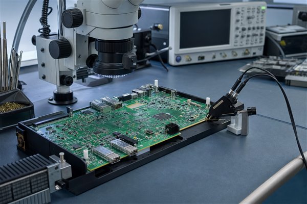
Match every quality gate to a risk, method, and record. Signal transmission PCB inspection must give the buyer evidence for each controlled characteristic. Visual appearance alone cannot prove controlled impedance, while a coupon measurement alone cannot prove assembly workmanship or complete channel compliance.
- Verify incoming materials. Check laminate, copper foil, thickness, lot identity, and approved substitutions. Provide the agreed material record or certificate of conformance.
- Inspect inner and outer conductors. Use AOI and dimensional process control to detect opens, shorts, neck-downs, over-etch, residual copper, and spacing errors. Retain the inspection status and required dimensional data.
- Check registration and plated holes. Evaluate layer alignment, annular rings, hole-wall quality, voids, and cracks with registration checks, X-ray where applicable, and microsection sampling. Supply the report when required by the purchase specification.
- Test electrical connectivity. Use flying-probe or fixture testing to find open circuits and unintended shorts. Record the tested revision and pass status.
- Measure controlled impedance. Test representative coupons or specified structures with TDR. The report should identify the target, tolerance, tested trace, layer structure, coupon, and result.
- Measure frequency-domain performance when specified. Use calibrated VNA and S-parameter methods to evaluate insertion loss, return loss, coupling, or mode conversion. Record fixtures, calibration, frequency range, and acceptance limits.
- Inspect assembly workmanship. Combine visual inspection, AOI, X-ray for hidden joints, and cleanliness testing as required. Record defects, rework, and nonconformance disposition.
- Run the functional interface test. Use the customer-approved procedure to check timing, protocol operation, eye performance, or intermittent faults. Record the procedure revision, limits, unit identity, and result.
- Complete the acceptance review. Confirm the required IPC revision, class, addenda, sampling plan, customer drawings, and approved exceptions before shipment.
TDR locates impedance changes over time or distance, but launches, coupons, cables, fixtures, calibration, and measurement windows affect results. VNA testing adds frequency-domain reflection and transmission data and also requires defined fixtures and calibration.
Applicable acceptance documents may include IPC-6012F for rigid-board performance, IPC-A-600M for printed-board acceptability, J-STD-001J for soldering process requirements, and IPC-A-610J for completed assembly acceptability. The purchase specification should identify the required revision, class, addenda, and customer-specific criteria.
What Signal Transmission PCB Design and Manufacturing Services Can We Provide?
Support must produce an approval or a verifiable deliverable. Founded in 2006, EBest Circuit supports signal transmission PCB projects from design and prototype through sourcing, assembly, and mass production.
| Service stage | Engineering work | Customer decision or deliverable |
| PCB design and DFM review | Review stackup, controlled nets, reference continuity, differential routing, via transitions, mask, test access, panelization, and conflicting notes | Resolved engineering questions and approved design changes before fabrication |
| Stackup coordination | Match requested materials and copper to available cores and prepregs; calculate producible widths and gaps | Approved production stackup and impedance geometry |
| Prototype fabrication | Build FR-4, high-speed, high-frequency, impedance-control, HDI, high-Tg, flexible, or rigid-flex prototypes as specified | Bare boards and the electrical, impedance, or inspection records named in the order |
| Component sourcing and PCB assembly | Review BOM, approved alternates, sourcing scope, centroid, stencil data, polarity, test access, programming, and handling requirements | Assembled boards with agreed inspection, programming, or functional-test records |
| Impedance verification | Test representative coupons against the released target, tolerance, layer, and structure | TDR report that identifies each tested impedance class |
| Production transfer | Preserve approved files, material rules, deviations, tests, and change approvals | Revision-controlled baseline for mass production and repeat orders |
| Expedited project review | Check stackup, material availability, quantity, assembly scope, testing, and shipping requirements | A committed schedule based on the actual build rather than a generic lead-time promise |
Define exclusions before quotation. Confirm whether pricing includes design work, component sourcing, fixtures, programming, impedance reports, X-ray, functional testing, packaging, and shipment documents. An unspecified service should not be assumed to be included.
Case Studies: FR4 Signal Transmission PCB Prototype to Mass Production
This is a representative FR-4 production-control scenario. It shows the decisions and records needed from prototype release through repeat production.
Project background: A multilayer FR-4 signal transmission PCB carries differential links, clocks, and mixed-signal interfaces through board-edge connectors. Prototype assembly precedes production release.
Project requirements: The release package identifies controlled nets, impedance targets and tolerances, layer references, component models, maximum pair skew, connector launches, prototype quantity, assembly data, and requested impedance evidence. It also states which material substitutions require approval.
Engineering review: The fabricator checks whether the proposed dielectric thickness and finished copper produce manufacturable widths and gaps. The review flags traces crossing reference voids, layer transitions without nearby return vias, excessive unused via stub, ambiguous solder-mask conditions, and test coupons that do not represent the routed structures.
Prototype controls: The approved stackup, geometry, material rules, coupon design, drill options, assembly drawings, and test procedure form one controlled package. Inspection separates bare-board evidence from assembly and functional results.
Production transfer: Approved revisions, material identity, coupon results, inspection records, and accepted deviations form the production baseline. Review laminate, copper, stackup, drill, component, stencil, or test changes before use.
Customer-verifiable outputs: Specify the approved stackup, resolved engineering questions, material record, electrical test status, impedance report, inspection results, assembly records, and functional data in the purchase specification.
Why Choose Us for Controlled-Impedance PCB Prototyping and Assembly?
Choose a supplier by the risk it removes from your project. EBest Circuit combines experience since 2006 with design, prototyping, sourcing, assembly, and mass-production support. Signal transmission PCB customers can reduce supplier handoffs while keeping technical approvals and acceptance evidence visible.
- Fewer engineering handoffs: One supplier can coordinate PCB design, prototype fabrication, component sourcing, assembly, and production transfer. This reduces revision mismatches between separate design, board, and assembly vendors.
- Relevant board technologies: FR-4, multilayer, high-speed, high-frequency, impedance-control, HDI, high-Tg, flexible, and rigid-flex options support different channel, density, thermal, and mechanical requirements.
- Prototype-to-production continuity: The approved stackup, engineering answers, coupon structures, inspection criteria, and accepted deviations can remain linked to the production revision. This lowers the risk of repeating an obsolete prototype decision.
- Quality evidence matched to the risk: Buyers can specify electrical testing, TDR reports, AOI, X-ray, programming, or functional testing instead of relying on a general quality claim.
- Support for regulated purchasing: EBest Circuit lists ISO 9001:2015, IATF 16949, ISO 13485:2016, AS9100D, UL, RoHS, and REACH support. Customers should confirm the current certificate or document, covered site, scope, and revision required for their order.
- Controlled changes after approval: Material, copper, stackup, geometry, drilling, components, stencil, or test changes can be reviewed before use. This protects signal-integrity assumptions and avoids unapproved substitutions.
- Practical urgent-build planning: Expedited options can be evaluated against material availability, quantity, assembly scope, testing, and shipping needs. Customers receive a project-specific commitment instead of an unsupported universal lead time.
Customer validation remains essential. Supplier records confirm conformance to released manufacturing requirements; they do not replace system simulation, protocol compliance, environmental qualification, or final product validation.
What Files and Specifications Are Required for a Signal Transmission PCB Quote?
A useful quote needs board, assembly, and test data. A complete signal transmission PCB quotation must identify the physical board, controlled structures, assembly scope, and verification plan. Missing stackup, impedance, or test information can produce a price that does not represent the intended build.
- Gerber or ODB++: Include every copper, solder-mask, legend, paste, profile, and mechanical layer with unambiguous layer names. This prevents missing layers, polarity errors, and artwork misinterpretation.
- NC drill files: Separate plated and non-plated holes and define slots, blind or buried vias, controlled-depth drilling, and backdrilling. This prevents the wrong via structure, residual stub, or mechanical mismatch.
- PCB stackup: State the layer order, finished copper, cores, prepregs, target dielectric thickness, material family, and permitted substitutions. These inputs are required for a valid impedance calculation.
- Controlled-impedance table: Identify each net class, single-ended or differential target, tolerance, routing layer, reference layer, mask condition, and coupon requirement.
- Fabrication drawing: Define board dimensions, finished thickness, copper, surface finish, solder mask, legend, profile, IPC revision and class, and special acceptance criteria.
- BOM and approved sources: Provide manufacturer part numbers, quantities, approved alternates, do-not-substitute parts, and sourcing responsibility. Highlight termination components and connectors that affect channel behavior.
- Centroid and assembly drawing: Include reference designators, X/Y coordinates, rotation, board side, polarity, special placement, and manual-assembly instructions.
- Test specification: Define the method, fixtures, limits, software, sample plan, calibration, report format, and customer-supplied test assets. State whether TDR, programming, functional testing, or interface validation is required.
- Commercial requirements: State prototype and production quantities, panel preference, delivery destination, packaging, revision, and requested schedule. This allows comparable pricing and lead-time review.
- Release status: Mark the package as design review or production release, list open decisions, and name the approval authority. This prevents unfinished data from being treated as approved production files.
Mark unfinished layouts as design-review releases and list open decisions. Do not treat a quote based on provisional impedance or material assumptions as production approval.
FAQs About Signal Transmission PCB
Q1: What impedance values are common on a signal transmission PCB?
A1: The interface specification and component guidance determine the required impedance. Single-ended and differential targets vary by protocol, connector, topology, and measurement reference. Do not copy a familiar value into the fabrication notes without identifying the controlled nets, tolerance, layers, and reference planes.
Q2: How should a signal transmission PCB impedance coupon represent production traces?
A2: The coupon should reproduce the controlled structure being accepted. Match the production layer, reference plane, dielectric construction, copper condition, mask condition, and relevant geometry. The drawing should identify which coupon trace corresponds to each impedance class.
Q3: What controlled-impedance tolerance should be specified?
A3: Set the tolerance from interface margin and measurement capability. A tighter number is not automatically better. Confirm whether the limit applies to nominal calculations, production coupons, or routed structures, and define the measurement method before ordering.
Q4: Why do PCB impedance calculators produce different results?
A4: They may use different equations, field solvers, material inputs, and geometry assumptions. Compare design Dk, pressed dielectric height, finished copper, plating, etched shape, solder mask, and frequency. Use the fabricator-approved stackup and correlate critical structures with a representative coupon.
Q5: Can a four-layer signal transmission PCB support controlled impedance?
A5: Yes, when the stackup provides a continuous nearby reference and producible geometry. Confirm dielectric height, finished copper, trace width, pair gap, plane continuity, and transitions with the fabricator. Layer count alone does not determine signal-integrity performance.
Q6: Why can prototype and production impedance results differ?
A6: Material, dielectric thickness, copper, etch, plating, resin flow, coupon design, and measurement setup can vary. Use the same approved construction, documented process controls, representative coupons, and change-approval rules to improve correlation.
Q7: Does length matching guarantee differential-pair signal integrity?
A7: No, length matching controls skew but does not correct impedance, loss, or return-path defects. The pair also needs symmetrical pads and vias, continuous reference planes, controlled coupling, suitable launches, and acceptable insertion and return loss.
Q8: Can a high-speed signal use a power plane as its reference?
A8: It can in a defined structure, but a continuous ground reference is usually easier to control. The power plane must remain continuous and provide a low-impedance high-frequency return relationship. If the reference changes, add an appropriate nearby return connection and validate the transition.
Q9: Does grounded copper beside a controlled trace change its impedance?
A9: Yes, nearby grounded copper can create coplanar coupling and shift the finished impedance. Define the copper gap, via stitching, mask condition, and keep-out in the field-solver model. Avoid uncontrolled or floating copper beside sensitive traces.
Q10: What should be checked after the fabricator changes trace width or pair spacing?
A10: Recheck more than the target impedance before approving the change. Verify clearance, differential coupling, delay, pair skew, pad neck-downs, solder mask, adjacent copper, routing density, and coupon geometry against the released stackup.
Conclusion
Reliability depends on preserving one controlled channel. A signal transmission PCB production release must preserve the approved stackup, geometry, return paths, transitions, assembly data, and acceptance evidence.
For a signal transmission PCB design review, controlled-impedance prototype, bare-board fabrication, PCB assembly, or production quotation, contact EBest Circuit at sales@bestpcbs.com. Send the Gerber or ODB++, NC drill, stackup, and impedance table. Include the fabrication drawing, quantity, BOM, centroid file, assembly drawing, and test requirements for engineering review before quotation.
You may also like


Tags: Signal Transmission PCB Assembly, Signal Transmission PCB Design, Signal Transmission PCB Prototype, Signal Transmission PCB Testing