





HDMI RF modulator component projects are used when HDMI video and audio need to be converted into an RF signal that can travel through coaxial cable to TVs, distribution systems, test equipment, or RF-based video networks. For buyers, the search is often about finding the right product or module. For engineers, the more practical question is whether the HDMI input, RF output, power circuit, shielding, connectors, and assembly process can work together reliably on a real PCB or PCBA.
EBest Circuit (Best Technology) supports PCB fabrication, component sourcing, SMT assembly, through-hole assembly, DFM review, inspection, testing coordination, and small-batch PCBA production for RF-related electronic products. If your HDMI RF modulator project already has Gerber files, BOM, CPL, stackup notes, connector drawings, or testing requirements, you can send them to sales@bestpcbs.com for an engineering review before production.
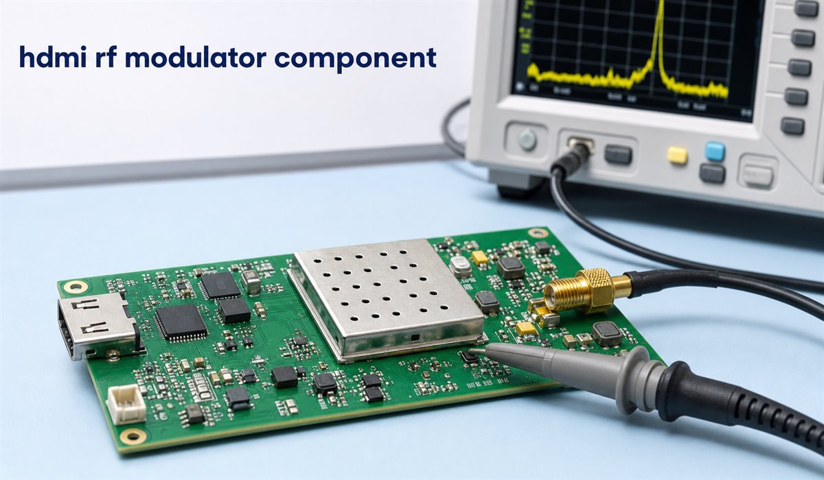
What Is an HDMI RF Modulator Component?
An HDMI RF modulator component is part of a circuit or module that helps convert an HDMI input signal into an RF output signal. In finished products, this function may appear inside an HDMI RF modulator box, an HDMI-to-coax converter, a video distribution device, or a custom RF video board.
In simple terms, the signal path usually starts from an HDMI input and ends at an RF output connector. Between these two points, the board may include video processing, modulation, clock control, power regulation, RF filtering, amplification, shielding, and output matching.
A typical HDMI RF modulator-related board may include:
- HDMI input connector
- ESD protection components
- HDMI receiver or video processing IC
- RF modulator IC or module
- Crystal or oscillator
- Power management circuit
- RF amplifier stage
- Filter network
- Shielding structure
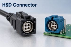
- Coaxial, F-type, or SMA connector
- Test points and programming interface
For PCB and PCBA work, the component itself is only one part of the project. The surrounding layout, stackup, grounding, impedance, connector mounting, soldering quality, and final testing often decide whether the assembled board works reliably.
How Does an HDMI to RF Modulator Component Work?
An HDMI to RF modulator component helps change a digital HDMI signal into an RF signal that can be distributed through coaxial cable.
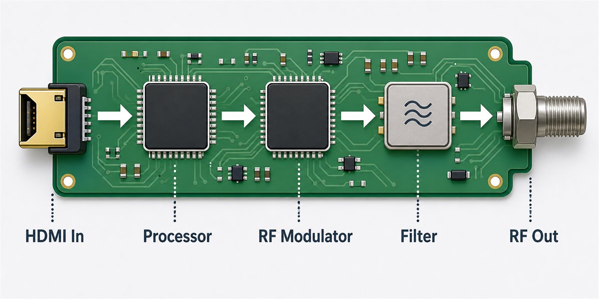
| Stage | Main Function |
| HDMI input | Receives video and audio |
| Processing IC | Handles signal conversion |
| Modulator | Creates RF output format |
| RF stage | Filters or amplifies signal |
| Output connector | Sends signal to coax system |
In a commercial HDMI RF modulator product, the circuit may support different output standards, channel settings, resolutions, or control functions. Those functions depend on the customer’s electronic design and selected chipset.
For EBest Circuit, the role is not to redefine the HDMI or RF design. The customer’s engineering team should define the circuit function, IC selection, modulation requirement, firmware, and RF performance target. Our role is to help confirm whether the approved PCB files, BOM, materials, assembly notes, and testing requirements can move into manufacturing with fewer avoidable risks.
This distinction matters. A circuit may be correct in theory, but problems can still appear during PCB fabrication or PCBA assembly if the connector footprint, RF trace, shielding pad, solder mask opening, grounding, or component package is not handled correctly.
Main Components Inside an HDMI RF Modulator Board
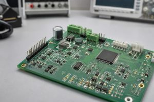
An HDMI RF modulator board usually combines digital video circuitry and RF circuitry on one assembly. That makes the manufacturing review more sensitive than a simple low-speed control board.
Key component groups usually include:
- HDMI interface parts: HDMI connector, ESD diodes, common-mode filters, input protection.
- Processing and modulation parts: HDMI receiver, video processing IC, RF modulator IC, memory, clock source.
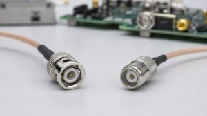
- RF output parts: RF amplifier, filter, matching network, coax connector, SMA connector, or F-type connector.
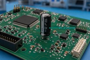
- Power parts: DC input connector, regulators, inductors, capacitors, ferrite beads, power filtering.
- Mechanical and shielding parts: shielding cans, connector shells, screws, mounting holes, enclosure contacts.
- Testing and control parts: test pads, programming pads, switches, LEDs, headers, communication interface.
The BOM should make critical choices clear:
- Exact HDMI connector model
- RF connector type and drawing
- IC package and footprint
- Substitute rules for RF components
- Impedance or RF path notes
- Shielding parts and soldering method
- Inspection and test requirements
If an HDMI connector or RF connector is changed during sourcing, the PCB footprint and assembly method may also need to be reviewed. A similar connector is not always a safe substitute.
RF HDMI Modulator Component PCB Layout and Signal Path
An RF HDMI modulator component project usually has two different signal worlds on the same PCB: high-speed digital HDMI signals and RF output signals.
The HDMI side may need controlled routing, ESD protection, short signal paths, and stable reference planes. The RF side may need 50 ohm routing, clean grounding, short matching paths, shielding, and a stable connector transition.
For manufacturing review, several areas deserve attention:
- HDMI connector footprint and soldering strength
- ESD component placement near the input
- RF output connector footprint
- Ground pad and via stitching around RF path
- Solder mask opening near RF pads
- Shielding can pad design
- Distance between noisy power circuits and RF path
- Board edge tolerance for edge or coax connectors
- Test point access after assembly
The PCB manufacturer should not change the customer’s RF layout without approval. However, the manufacturer should check whether the design files are clear enough for production.
For example, if the RF connector drawing requires a specific board thickness, plating area, solder mask clearance, or mechanical keepout, those details should be visible before fabrication starts. If the shielding can needs solderable pads, those pads must match the real component and assembly process.
50 Ohm Routing for HDMI RF Modulator Component Boards
Many HDMI RF modulator component boards require 50 ohm control on the RF output path. The actual requirement should come from the customer’s RF design file, impedance note, or connector/module datasheet.
| Factor | Why It Matters |
| Trace width | Affects impedance |
| Dielectric thickness | Changes RF field geometry |
| Copper thickness | Affects finished trace |
| Reference plane | Provides return path |
| Solder mask | May affect RF trace slightly |
| Connector launch | Affects transition quality |
| Ground vias | Help stabilize RF return |
For lower-frequency or less sensitive products, carefully controlled FR4 may be acceptable. For higher-frequency, low-loss, or more demanding RF products, the material may need closer review. Some projects may require RF laminate, high-Tg FR4, hybrid stackup, or tighter impedance confirmation.
EBest Circuit can review stackup, copper thickness, material, impedance notes, and RF connector area before production. If the customer requires an impedance coupon or impedance test report, that should be planned before fabrication, not added after the board is already made.
4K HDMI to RF Modulator Component Manufacturing Checks
A 4K HDMI to RF modulator component board usually has tighter expectations than a basic video converter. Even when the PCB manufacturer is not responsible for the video algorithm or product design, the board still needs stable fabrication and assembly control.
For a 4K modulator related project, customers may care about signal stability, heat control, HDMI connector reliability, RF output consistency, shielding effectiveness, power noise reduction, firmware access, production repeatability, and final functional test method.
Important manufacturing questions include:
- Is the HDMI connector footprint correct?
- Are fine-pitch ICs suitable for the SMT process?
- Are QFN, BGA, or exposed-pad components handled correctly?
- Is the RF output path protected from unnecessary process variation?
- Is the board thickness suitable for connectors and enclosure?
- Are shielding cans, thermal pads, and test points accessible?
- Are programming and functional testing steps defined before shipment?
A 4K product can fail for many reasons, including firmware, chipset selection, signal standard, or system-level compatibility. PCB and PCBA problems should not be added to that risk. Clean files, controlled fabrication, accurate SMT, and practical testing help make the first build easier to evaluate.
8 Channel HDMI RF Modulator Component PCB and PCBA Needs
An 8 channel HDMI RF modulator component project may involve more connectors, more heat, more RF paths, and more assembly risk than a single-channel board.
Compared with a one-channel design, an 8-channel board may need stronger attention to:
- Connector spacing
- Channel-to-channel isolation
- Shielding arrangement
- Power distribution
- Thermal spreading
- RF output routing
- Enclosure alignment
- Test coverage
- Labeling and packing
The board may include multiple HDMI inputs, multiple processing sections, RF output circuits, and control interfaces. Even if the circuit is modular, the PCBA still needs stable production handling.
For this type of project, panelization and inspection planning become important. A larger or denser board should be reviewed for warpage, connector stress, SMT support, and test access. If the product uses many HDMI connectors or coax connectors, mechanical strength and solder joint reliability should be checked carefully.
For small-batch production, customers often need more than bare PCB fabrication. They may need component sourcing, SMT assembly, manual soldering, connector assembly, testing, packing, and documentation under one workflow. That is where a one-stop PCB and PCBA supplier can reduce communication gaps.
BOM Sourcing and SMT Assembly for HDMI RF Modulator Components
BOM sourcing is often one of the biggest risks in HDMI RF modulator component projects. Some parts may have similar names but different packages, footprints, frequency ranges, temperature ratings, or mounting requirements.
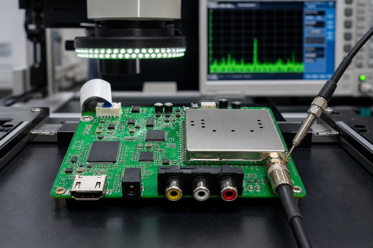
Before SMT, the BOM should confirm:
- Exact HDMI connector model
- Exact RF connector model
- Modulator IC or module part number
- Crystal or oscillator specification
- Regulator current rating
- RF filter and matching parts
- Shielding can model
- Package size for all fine-pitch parts
- Approved alternate components
- Customer-supplied or supplier-sourced parts
- Testing and programming notes
SMT assembly also needs practical attention. HDMI connectors, QFN packages, RF shields, exposed-pad ICs, small passives, and coax connectors may require different process controls.
Typical PCBA checks include:
- Solder paste printing
- SPI
- Pick-and-place accuracy
- Reflow profile
- AOI inspection
- X-Ray when needed
- Manual soldering for selected connectors
- Cleaning requirements
- Functional test coordination
- Final packing protection
EBest Circuit supports both PCB fabrication and PCBA assembly, so the same project notes can stay visible from file review to shipment. This is useful when a board includes mixed requirements such as HDMI interface, RF path, shielding, SMT, through-hole connectors, and functional testing.
HDMI RF Modulator Component Manufacturing Case Study
A European customer needed a small-batch PCBA build for an HDMI-to-RF video distribution module used in a commercial display system. The project was not a simple bare PCB order. It included HDMI input, RF output, fine-pitch components, shielding requirements, connector assembly, and functional test notes.
Project background:
- Customer region: Europe
- Application: commercial video distribution module
- Build type: PCB fabrication, component sourcing, and PCBA assembly
- Quantity: 80 pcs pilot batch
- PCB type: 4-layer FR4 PCB
- Surface finish: ENIG
- Key areas: HDMI input connector, RF output connector, shielding can area, power section
- Assembly: SMT plus selected manual connector soldering
- Testing: visual inspection, AOI, connector inspection, basic power-on and signal-path test coordination
Main manufacturing risks:
- HDMI connector solder joints needed stable mechanical strength.
- RF output path required controlled layout and clean grounding.
- Shielding pads had to be solderable and accessible.
- Several components had similar package options, so BOM confirmation was important.
- The customer needed pilot-build feedback before moving to the next batch.
EBest Circuit support:
- Reviewed Gerber, BOM, CPL, stackup, and assembly drawing together.
- Checked HDMI and RF connector footprints against the supplied drawings.
- Confirmed RF path notes, ground pads, shielding pads, and solder mask openings.
- Reviewed BOM availability and suggested confirmation on risky component alternatives.
- Arranged SMT assembly and connector-related process control.
- Kept testing and packing notes visible until final shipment.
Result:
The customer received a pilot batch ready for engineering validation. The value of the project was not only that the boards were assembled. The value was that connector mounting, RF path handling, BOM sourcing, SMT assembly, inspection, and testing notes were managed together before the customer started system-level evaluation.
For HDMI RF modulator products, this kind of coordination can reduce avoidable delays between prototype build, debugging, customer approval, and small-batch production.
FAQs About HDMI RF Modulator Component
1. What is an HDMI RF modulator component?
An HDMI RF modulator component is a part, module, or circuit section that helps convert HDMI video/audio signals into RF output for coaxial distribution or RF-based video systems.
2. Is an HDMI RF modulator component the same as an HDMI RF modulator box?
No. An HDMI RF modulator box is a finished product. An HDMI RF modulator component may be one part of the internal circuit, module, or PCBA used inside that product.
3. Does an HDMI RF modulator component board need 50 ohm routing?
Many RF output paths need 50 ohm routing, but the exact requirement should come from the customer’s RF design, module datasheet, or impedance note.
4. Can EBest Circuit design the HDMI RF modulator circuit?
EBest Circuit focuses on PCB fabrication, PCB layout manufacturability review, component sourcing, PCBA assembly, inspection, and testing support. The HDMI/RF circuit design, chipset selection, and firmware logic should come from the customer’s design team.
5. What files are needed for HDMI RF modulator component PCBA production?
Useful files include Gerber or ODB++, BOM, CPL, stackup, assembly drawing, connector drawings, impedance notes, shielding notes, testing requirements, and packing instructions.
All in all, an HDMI RF modulator component project is not only about selecting one electronic part. The real production risk is whether the HDMI input, RF output, PCB stackup, connectors, BOM, SMT assembly, shielding, and testing steps can work together. If you are preparing an HDMI RF modulator board or PCBA project, please send your Gerber files, BOM, CPL, connector drawings, and project notes to sales@bestpcbs.com. EBest Circuit can help review the manufacturing path before production begins.
You may also like

Tags: hdmi rf modulator, hdmi rf modulator component, rf modulator pcb