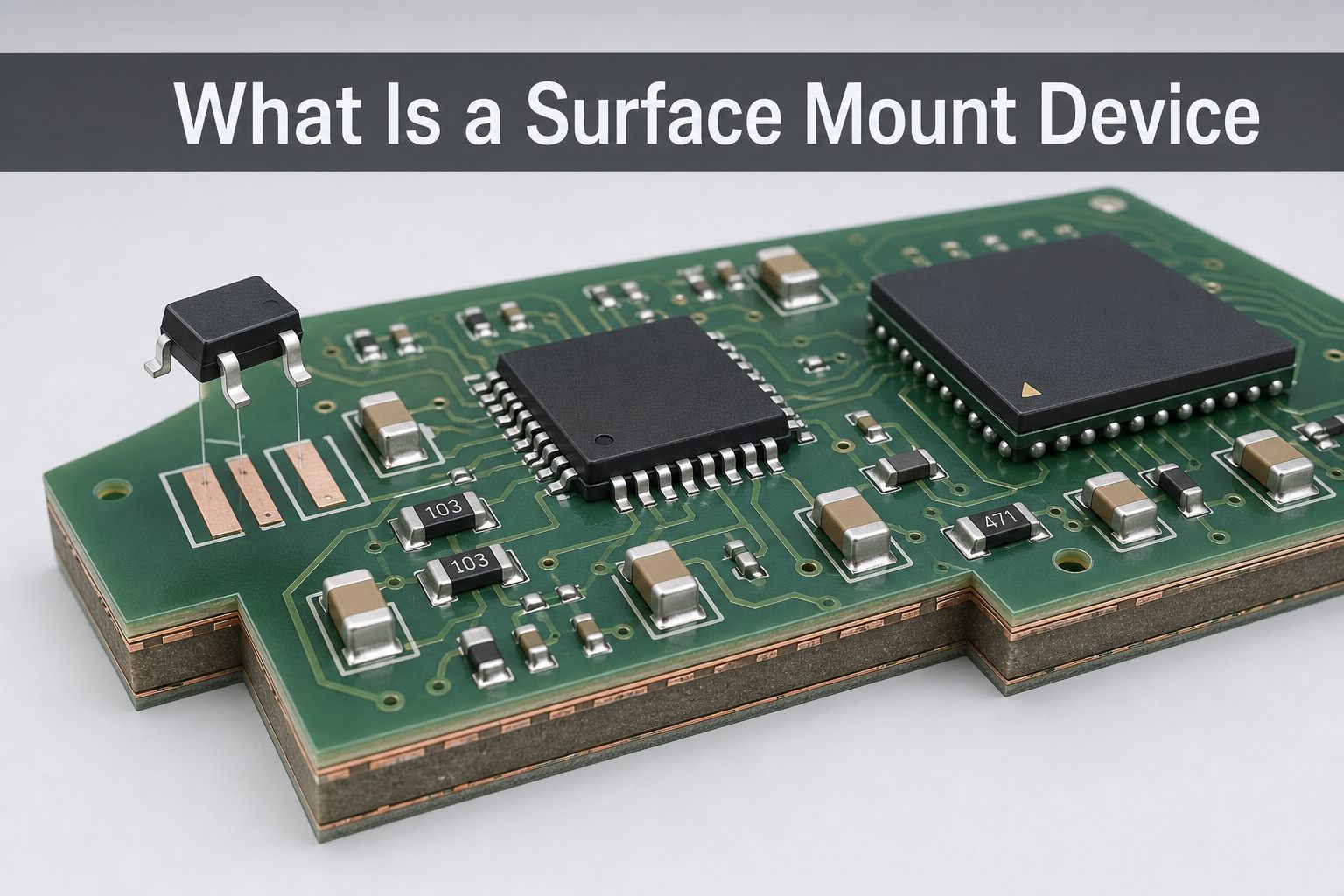
A surface mount device (SMD) is an electronic component designed to be soldered directly onto copper lands on the surface of a printed circuit board. Unlike a through-hole part, its terminals normally do not pass through plated holes. SMDs include chip resistors, capacitors, diodes, transistors, LEDs, sensors, connectors and integrated circuits.
The definition is simple, but selecting an SMD is also a manufacturing decision. The package must match the PCB footprint, polarity and pin-one data must agree across the schematic, BOM and pick-and-place file, and the assembly process must be able to print, place, reflow and inspect the resulting joints.
What Is a Surface Mount Device?
A surface mount device is the physical electronic part that an SMT line places and solders onto PCB surface pads. Its electrical terminals may be metal end caps, gull-wing leads, J-leads, flat pads, exposed thermal pads or solder balls, depending on the package.
The term describes the mounting format, not the electrical function. A resistor, MOSFET, microcontroller and connector can all be SMDs even though they perform very different jobs. The common feature is that the package is intended for surface attachment and must be paired with a compatible PCB land pattern.
How Is an SMD Different from SMT and Through-Hole Components?
SMD is the component, SMT is the assembly technology, and through-hole describes parts whose leads are inserted through drilled holes. The terms are related but not interchangeable.
| Term | What It Means | Main Design Concern |
| SMD | The surface-mount component | Package, pinout, polarity, thermal pad and availability |
| SMT | The process used to assemble SMDs | Solder paste, placement, reflow and inspection |
| Through-hole | A component with leads inserted through PCB holes | Hole size, annular ring, insertion and mechanical support |
Many production PCBAs use mixed assembly. Small passives and ICs are commonly surface mounted, while some connectors, transformers, switches or mechanically loaded parts may remain through-hole. The correct choice depends on electrical, thermal, mechanical and service requirements rather than package size alone.
What Are the Common Surface Mount Device Package Types?
Common surface mount device package types range from two-terminal chip parts to fine-pitch and bottom-terminated ICs. The package name identifies a physical family, but the exact dimensions and pin mapping must still be confirmed in the manufacturer datasheet.
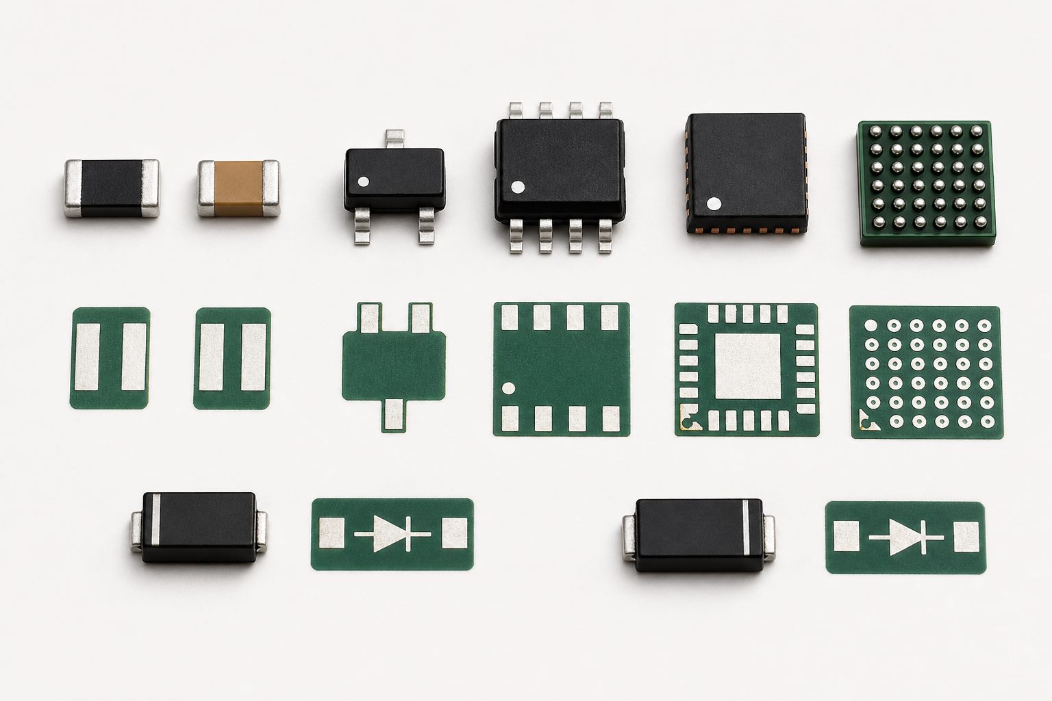
| Package Family | Typical Parts | Assembly Attention |
| Chip packages such as 0402, 0603 and 0805 | Resistors, capacitors and inductors | Paste balance, placement accuracy and tombstoning risk |
| SOT and SOD | Transistors, regulators and diodes | Pinout and polarity or orientation marks |
| SOIC, TSSOP and QFP | Integrated circuits | Lead pitch, coplanarity, paste control and bridge inspection |
| QFN and DFN | ICs and power devices | Exposed-pad paste coverage and hidden perimeter joints |
| BGA and LGA | Processors, memory and modules | Land design, warpage, reflow control and X-ray inspection |
| PLCC and SMD LED packages | LEDs and selected ICs | Polarity, thermal path and optical orientation |
A label such as 0603 can be ambiguous because imperial and metric naming systems use different dimensions. Put the manufacturer part number and package dimensions in the BOM instead of relying only on a short package code.
How Do You Match an SMD Package to a PCB Footprint?
Reliable SMD footprint design starts with the exact component datasheet and its recommended land pattern, not with a visually similar library name. Compare package body size, terminal dimensions, pitch, exposed-pad geometry, pin numbering and the datasheet revision before releasing the layout.
IPC-7351 provides generic requirements for surface-mount design and land patterns, including considerations for solder joints, inspection and rework. A generic standard does not replace a component-specific recommendation; use both where applicable and confirm the assembly supplier’s process capabilities.
- Verify the manufacturer part number against the schematic symbol and BOM.
- Check pad length, width, pitch and solder-mask clearances.
- Confirm paste apertures for exposed pads and fine-pitch leads.
- Keep a suitable component courtyard for placement, inspection and rework.
- Check pin one, cathode, positive terminal and package rotation conventions.
- Review thermal vias and copper spreading for power packages.
A footprint can be electrically correct yet difficult to manufacture. Large paste deposits may void or float a bottom-terminated package, undersized pads can reduce solder fillets, and crowded courtyards can block inspection or rework access.
Why Do SMD Polarity Markings and Orientation Matter?
SMD polarity markings and pin-one indicators prevent electrically asymmetric parts from being assembled in the wrong direction. Diodes, LEDs, polarized capacitors and most ICs require consistent orientation data, while ordinary resistors and many ceramic capacitors are non-polarized.
Do not assume every package uses the same dot, stripe, notch or chamfer convention. Read the component datasheet, then make the schematic symbol, PCB footprint, silkscreen, assembly drawing and centroid rotation agree. The BOM should identify the exact manufacturer part number so an alternate package is not substituted without review.
Before fabrication, compare a top-view package drawing with the top-view PCB footprint. This simple check catches mirrored footprints, transposed pins and ambiguous polarity marks before they become an assembled-board failure.
How Does Surface Mount Device Assembly Work?
Surface mount device assembly normally follows solder paste printing, automated placement, controlled reflow and inspection. Each stage depends on correct design data from the previous stage.

- A laser-cut stencil deposits solder paste on the PCB pads.
- Feeders present parts from reels, tubes or trays to the placement machine.
- Pick-and-place nozzles identify, orient and place each SMD from centroid data.
- The reflow oven heats the assembly according to the solder paste and component limits.
- AOI checks visible placement and solder-joint conditions.
- X-ray inspection may be used for BGA, QFN, LGA and other hidden joints.
- Electrical or functional testing checks whether the assembled circuit operates as required.
BestPCBs provides PCB assembly and PCBA support that includes component sourcing, SMT and mixed assembly, inspection and testing. If paste volume requires special control, the related SMT stencil service can support framed, unframed and stepped stencil requirements.
Which Files Are Needed for SMD PCB Assembly?
A manufacturer needs synchronized design and purchasing data to assemble SMDs correctly. At minimum, prepare fabrication data, a BOM, centroid or pick-and-place data and an assembly drawing.
- Gerber or ODB++ files for PCB fabrication
- BOM with manufacturer part number, description, quantity and package
- Pick-and-place file with reference designator, X/Y location, side and rotation
- Assembly drawing with pin-one and polarity information
- Stencil or paste-layer data
- Approved alternates and do-not-substitute restrictions
- Programming, test and special handling instructions
Run a cross-check before quotation: every placed reference designator should exist in the BOM, every BOM line should map to the intended footprint, and every polarized part should have an unambiguous orientation. The custom PCB assembly checklist provides a broader handoff path for prototype and production builds.
What Surface Mount Device Quality Problems Should You Check?
Common SMD assembly problems include wrong parts, reversed polarity, component shift, tombstoning, solder bridges, insufficient solder, open joints and hidden-joint voiding. Inspection should be selected according to the package and the visibility of its connections.
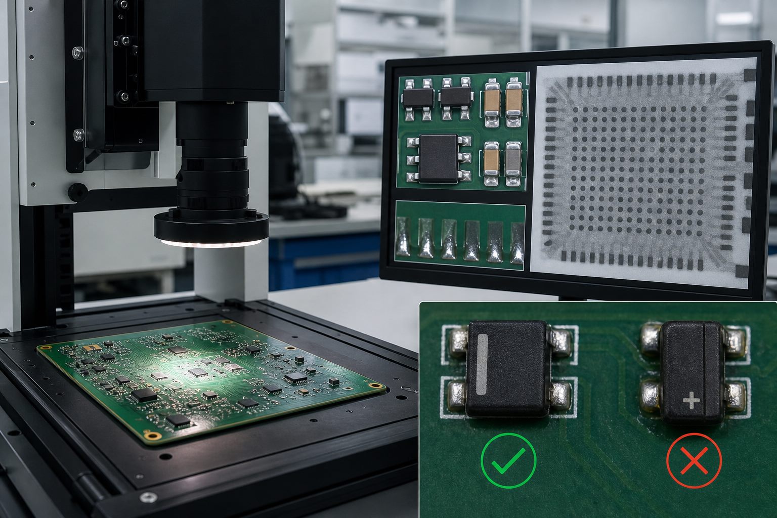
| Risk | Typical Check | Design or Process Response |
| Wrong or reversed component | BOM verification, AOI and functional test | Clear part number, polarity and rotation data |
| Tombstoned chip component | AOI or visual inspection | Balanced pads, paste deposits and thermal conditions |
| Bridged fine-pitch leads | AOI and electrical test | Review land pattern, stencil aperture and reflow process |
| Open or insufficient joint | AOI, visual inspection or electrical test | Check paste transfer, coplanarity and wetting surfaces |
| Hidden BGA or QFN concern | X-ray and functional test | Review pad geometry, paste segmentation and reflow profile |
Moisture-sensitive semiconductor packages also need controlled storage and floor-life handling. Moisture trapped inside a package can expand during reflow and cause internal damage; check the component’s moisture sensitivity level, packaging label and applicable handling instructions before assembly.
How Do You Choose a Surface Mount Device for Production?
The best production choice is the SMD that meets electrical requirements while remaining available, inspectable and compatible with the intended assembly process. The smallest package is not automatically the lowest-risk or lowest-cost option.
- Electrical: voltage, current, tolerance, frequency, leakage and noise.
- Thermal: power dissipation, junction temperature, exposed pad and PCB heat path.
- Mechanical: package dimensions, board flex, vibration and connector loading.
- Manufacturing: pitch, stencil release, placement accuracy, rework and inspection access.
- Supply chain: lifecycle status, approved sources, lead time and qualified alternates.
- Documentation: reliable datasheet, land pattern, 3D model and traceable part number.
For an early prototype, a slightly larger leaded package may reduce hand-assembly and rework difficulty. For volume production, a smaller bottom-terminated package may save area and improve electrical or thermal performance, but it can require tighter paste control and X-ray access. Review the trade-off with the assembler before freezing the layout.
Frequently Asked Questions About Surface Mount Devices
Are all SMD components polarized?
No. Resistors and many ceramic capacitors are non-polarized. Diodes, LEDs, polarized capacitors and most integrated circuits require a defined orientation. Always use the datasheet rather than guessing from package shape.
Can a surface mount device be soldered by hand?
Many larger SMD packages can be hand-soldered for prototypes or repair with suitable tools and magnification. Fine-pitch, bottom-terminated and very small packages are more repeatable with controlled paste printing, placement and reflow.
What does 0603 mean on an SMD package?
It is a size code, but it can refer to different dimensions in imperial and metric systems. Confirm the actual body dimensions in the component datasheet and state the full manufacturer part number in the BOM.
Does an SMD need drilled component holes?
Normally no. Its terminals attach to surface lands. A PCB can still contain vias, tooling holes and through-hole parts elsewhere, and some special surface-mount packages include mechanical locating features.
Are QFN and BGA components SMDs?
Yes. Both are surface-mount package families. Their solder joints are partly or fully underneath the body, so land design, paste control, reflow and X-ray inspection deserve special attention.
Can two components with the same value use different footprints?
Yes. The same electrical value can be sold in multiple package sizes and pin configurations. A substitute is acceptable only when electrical ratings, package dimensions, pinout, thermal behavior and manufacturing constraints are all compatible.
Why are many SMDs supplied on tape and reel?
Tape-and-reel packaging protects component orientation and lets automated feeders present parts consistently to a pick-and-place machine. Tubes and trays are also common for larger or specialized packages.
What is MSL for a surface mount device?
Moisture Sensitivity Level defines handling precautions and allowable exposure conditions for moisture-sensitive packages before reflow. Follow the package label, manufacturer guidance and the applicable handling standard.
Which inspection method is used for SMD solder joints?
AOI is useful for visible placement and joint conditions. X-ray is commonly considered for hidden joints under BGA, QFN and similar packages. Electrical and functional tests confirm circuit behavior that visual inspection cannot prove.
What should be checked before approving an SMD alternate?
Check function, ratings, pinout, package dimensions, land-pattern compatibility, polarity, thermal needs, lifecycle status and assembly implications. Document the approved alternate in the BOM instead of allowing an uncontrolled substitution.
Summary
A surface mount device is a component made for direct attachment to PCB surface lands, but a production-ready choice requires more than identifying an SMD package. Match the exact part to its footprint, control orientation and moisture handling, provide synchronized assembly files, and plan inspection around visible or hidden solder joints.
If you are preparing a surface mount device assembly project, send your Gerber files, BOM, pick-and-place data, quantity and test requirements to sales@bestpcbs.com. The EBest Circuit engineering team can review the package-to-footprint handoff and provide a PCB/PCBA manufacturing quotation.
You may also like



Tags: SMD footprint design, SMD polarity markings, surface mount device assembly, surface mount device package types, what is a surface mount device