





A full wave rectifier converts both halves of an alternating-current waveform into a unidirectional output. Compared with a half wave rectifier, it produces a higher average DC voltage, doubles the ripple frequency, and makes downstream filtering easier.
The two common circuit arrangements are the center-tapped rectifier and the bridge rectifier. Both produce pulsating DC rather than perfectly stable DC, so most practical power supplies add a reservoir capacitor, regulator, or additional filter stage.
For a classroom circuit, understanding the diode current path may be enough. For a production full wave rectifier PCB, engineers must also evaluate diode losses, transformer regulation, capacitor ripple current, startup surge, copper temperature rise, safety spacing, and test access.
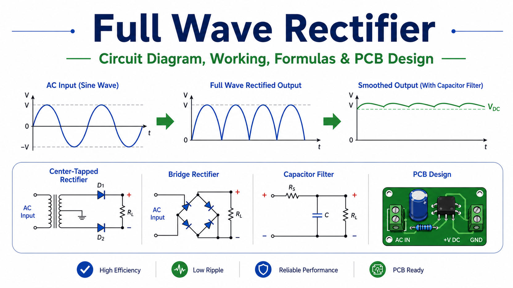
What Is a Full Wave Rectifier?
A full wave rectifier is an AC-to-DC conversion circuit that uses both the positive and negative half-cycles of an AC input. The diodes redirect current so it always passes through the load in the same direction.
The output is pulsating DC. It remains above the zero reference, but its voltage rises and falls with each rectified half-cycle. A filter capacitor can smooth these variations, while a voltage regulator can provide a more stable final output.
Full-wave rectification is widely used in:
- Linear power supplies
- Battery chargers
- Audio amplifier power stages
- Industrial control boards
- Appliance power modules
- Instrumentation equipment
- Low-voltage transformer supplies
- Motor-control DC buses
The topology should be selected according to transformer configuration, output voltage, load current, acceptable power loss, component cost, and PCB area.
How Does a Full Wave Rectifier Circuit Work?
A full wave rectifier circuit diagram usually includes an AC source or transformer secondary, rectifier diodes, a load, and an optional filter capacitor.
During the positive half-cycle, one diode path becomes forward-biased and carries current through the load. During the negative half-cycle, another path conducts. Although the AC polarity changes, the diode arrangement keeps the load-current direction unchanged.
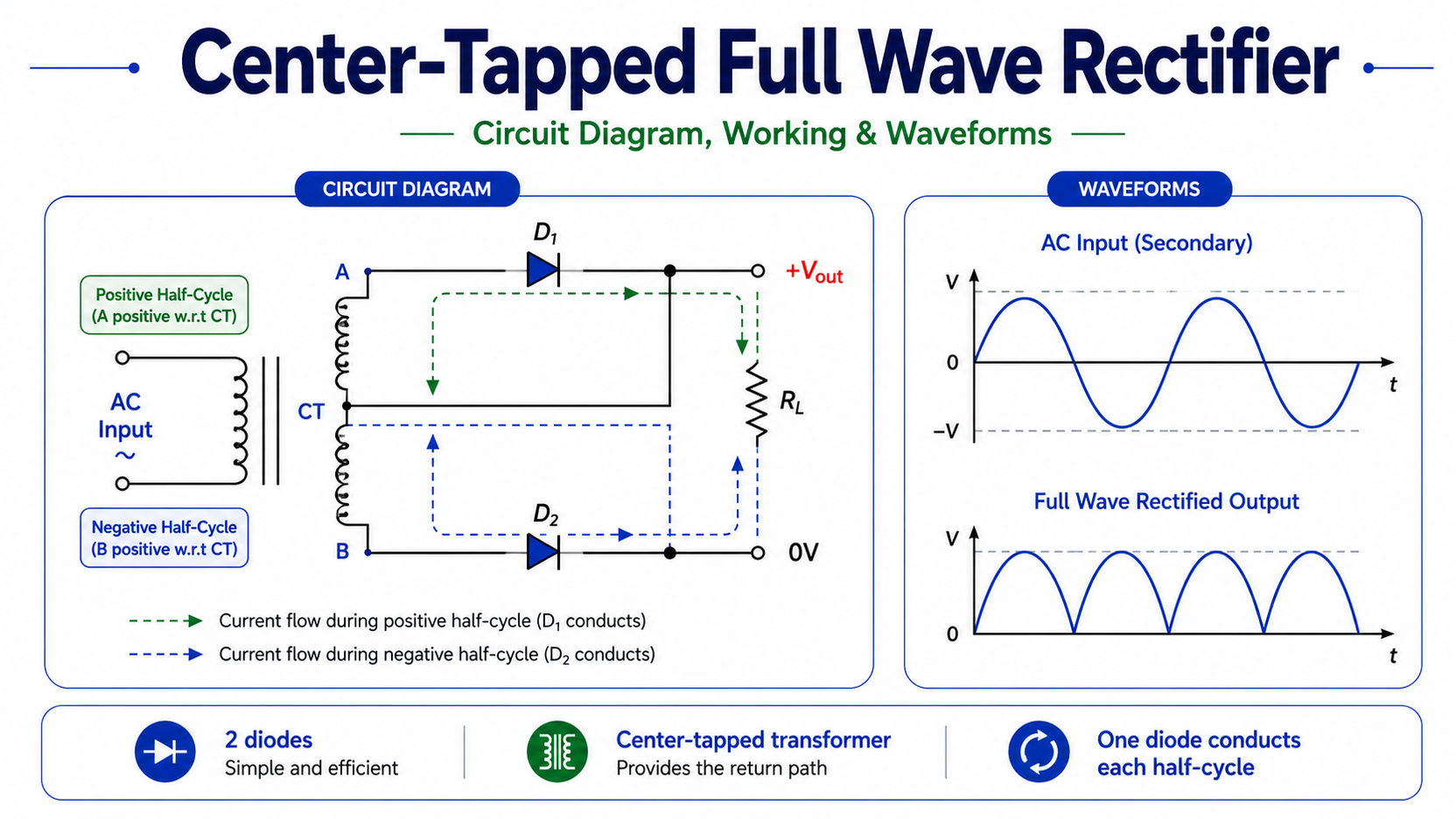
In a center-tapped circuit, one diode conducts during each half-cycle. In a bridge circuit, two diodes conduct in series during each half-cycle.
This difference affects the practical output voltage.
Here, VF is the forward voltage of one conducting diode, VSEC(PEAK) is the peak voltage of the complete bridge input winding, and VHALF(PEAK) is the peak voltage of one half of a center-tapped secondary.
A silicon rectifier diode may drop approximately 0.6 to 1.1 V under load. The exact value depends on current, junction temperature, diode construction, and package size. Datasheet curves should therefore be used for practical calculations.
What Are the Two Types of Full Wave Rectifiers?
The two standard types are the center-tapped full wave rectifier and the bridge full wave rectifier.
A center-tapped rectifier uses two diodes and a transformer secondary with a center connection. Each half of the secondary winding supplies the load on alternating half-cycles. Only one diode is in the active current path, which helps reduce forward-voltage loss.
A bridge full wave rectifier uses four diodes. Two conduct during the positive half-cycle, and the other two conduct during the negative half-cycle. It uses the complete transformer secondary during both half-cycles and does not require a center tap.
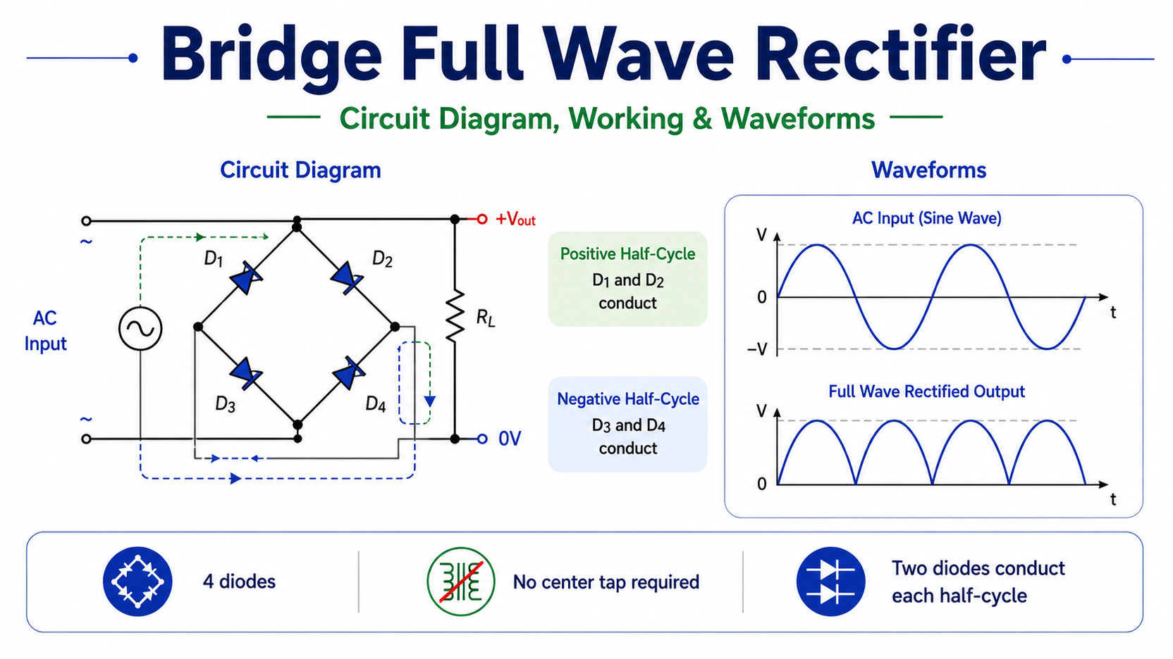
Bridge circuits are more common in general-purpose AC-to-DC power supplies because standard two-wire transformers are widely available. Center-tapped designs remain useful when the transformer already provides the required winding, when one diode drop is preferable, or when the circuit needs split positive and negative supply rails.
Rectification can be implemented with four discrete diodes or a single bridge package. Discrete diodes provide more flexibility in package selection, thermal spreading, and diode technology. An integrated bridge reduces placement count and simplifies assembly, but its current rating still depends heavily on package temperature and PCB heat dissipation.
Center-Tapped vs Bridge Full Wave Rectifier: What Is the Difference?
A bridge rectifier is one form of full-wave rectification. The technically useful comparison is therefore between a center-tapped full wave rectifier and a bridge full wave rectifier.
| Design factor | Center-tapped rectifier | Bridge rectifier |
|---|---|---|
| Number of diodes | 2 | 4 |
| Diodes conducting per half-cycle | 1 | 2 |
| Transformer requirement | Center-tapped secondary | Standard two-wire secondary |
| Secondary winding used per half-cycle | Half of the winding | Complete winding |
| Forward-voltage loss | One diode drop | Two diode drops |
| Typical diode PIV requirement | About twice the half-winding peak | About the full-winding peak |
| Transformer utilization | Lower | Higher |
| Rectifier component count | Lower | Higher |
| Transformer availability | More specialized | Generally easier to source |
| Low-voltage performance | Lower diode loss | Higher diode loss |
| Typical use | Split supplies, legacy linear supplies | General AC-to-DC conversion |
The bridge circuit is usually the practical default because it uses a conventional transformer and makes better use of the secondary winding.
However, diode loss becomes significant in low-voltage, high-current supplies. Losing 1.4 V across a bridge has limited impact on a 24 V output but represents a large efficiency penalty in a 5 V rail. Schottky diodes, a center-tapped design, or synchronous rectification may be more appropriate in that situation.
What Does a Full Wave Rectifier Waveform and Output Look Like?
The AC input waveform alternates above and below zero. After full-wave rectification, the negative half-cycle is inverted, so both halves appear with the same polarity at the load.
The raw full wave rectifier waveform reaches a peak and then falls toward zero during every half-cycle. Its ripple frequency is twice the AC source frequency:
- A 50 Hz AC input produces 100 Hz ripple.
- A 60 Hz AC input produces 120 Hz ripple.
When a reservoir capacitor is connected across the output, it charges near the waveform peak. It then supplies current to the load while the rectified input falls. The result is a DC voltage with a smaller sawtooth-like or curved ripple rather than a waveform that repeatedly returns to zero.
Consider a transformer secondary rated at 12 V RMS:
After a silicon bridge, the theoretical no-load capacitor voltage may approach 16.97 V minus two diode drops. The measured voltage under load will normally be lower because of transformer winding resistance, transformer regulation, diode forward loss, capacitor ripple, load current, mains-voltage variation, capacitor ESR, and PCB resistance.
Power-supply verification should include minimum and maximum AC input, no load, normal load, and peak load. Checking only the nominal transformer voltage can lead to insufficient regulator headroom at low line or excessive capacitor voltage at high line.
What Are the Main Full Wave Rectifier Formulas?
The standard full wave rectifier formulas assume a sinusoidal input, ideal diodes, and a resistive load unless stated otherwise.
| Parameter | Formula | Application |
|---|---|---|
| Average DC output | VDC = 2Vm / π | Average value of an unfiltered full-wave waveform |
| Approximate average DC output | VDC = 0.637Vm | Simplified numerical form |
| RMS output voltage | VRMS = Vm / √2 | Heating-equivalent voltage for a resistive load |
| Average DC load current | IDC = VDC / RL | Average load current |
| Ripple frequency | fr = 2finput | Full-wave output repetition rate |
| Ideal unfiltered ripple factor | r = 0.482 | AC content relative to the DC component |
| Maximum ideal efficiency | η ≈ 81.2% | Theoretical rectification efficiency |
| Center-tapped diode PIV | PIV ≈ 2Vm | Reverse stress when Vm is one half-winding peak |
| Bridge diode PIV | PIV ≈ Vm | Reverse stress when Vm is the bridge-input peak |
The frequently quoted 81.2% value is an ideal limit for an unfiltered full wave rectifier with a resistive load. It is not the efficiency of the complete power supply.
A real design must also include transformer copper and core losses, diode conduction loss, capacitor ESR loss, regulator loss, PCB conductor loss, and standby consumption.
The formula 2Vm/π describes the average of an unfiltered rectified sine wave. It should not be used as the final DC output of a capacitor-input supply, where the capacitor charges closer to the waveform peak.
How Does a Full Wave Rectifier with a Capacitor Filter Work?
A capacitor filter stores energy near each rectified voltage peak. When the input voltage rises above the capacitor voltage, the diodes conduct and recharge it. When the input falls below the capacitor voltage, the diodes stop conducting and the capacitor supplies the load.
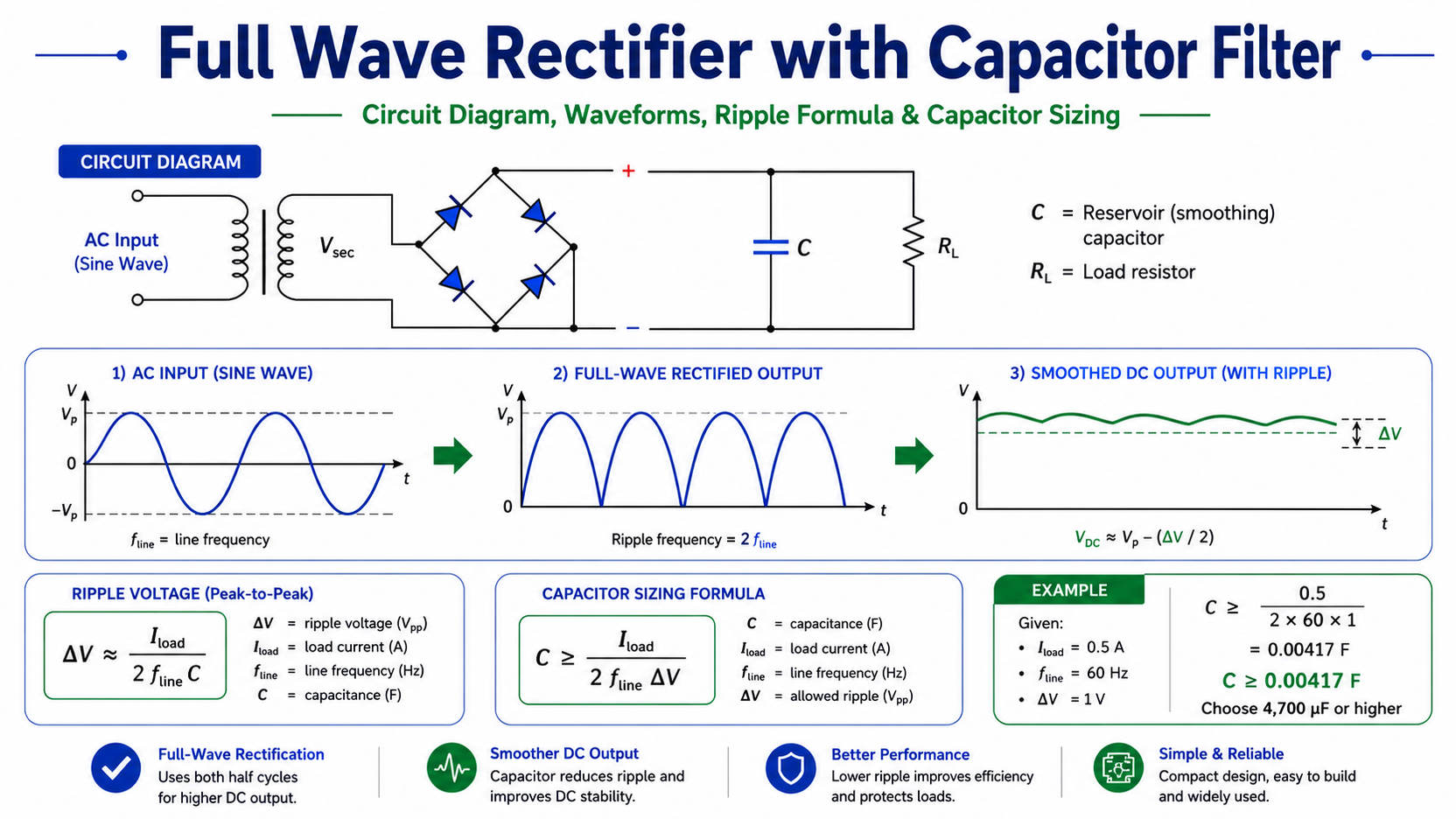
For a 60 Hz supply delivering 0.5 A with a maximum target ripple of 1 V, the calculated minimum is approximately 0.00417 F. A 4,700 µF capacitor would be a reasonable initial value.
The final choice should also account for:
- Voltage rating above the highest no-load DC voltage
- Ripple-current capability
- Service life at the expected internal temperature
- ESR at the operating frequency
- Capacitance tolerance and aging
- Mechanical dimensions and lead spacing
- Polarity and assembly access
- Startup inrush
A larger capacitor reduces voltage ripple but creates shorter and higher charging-current pulses. These pulses increase diode RMS current, transformer heating, electromagnetic noise, and startup stress.
For this reason, capacitance should not be increased without checking the bridge, transformer, fuse, connector, and PCB current path. Applications requiring tightly regulated voltage normally add a linear regulator, switching regulator, LC filter, or active power stage after the reservoir capacitor.
Half-Wave vs Full-Wave Rectifier: What Is the Difference?
The main selection factors are load power, allowable ripple, transformer utilization, and acceptable circuit complexity.
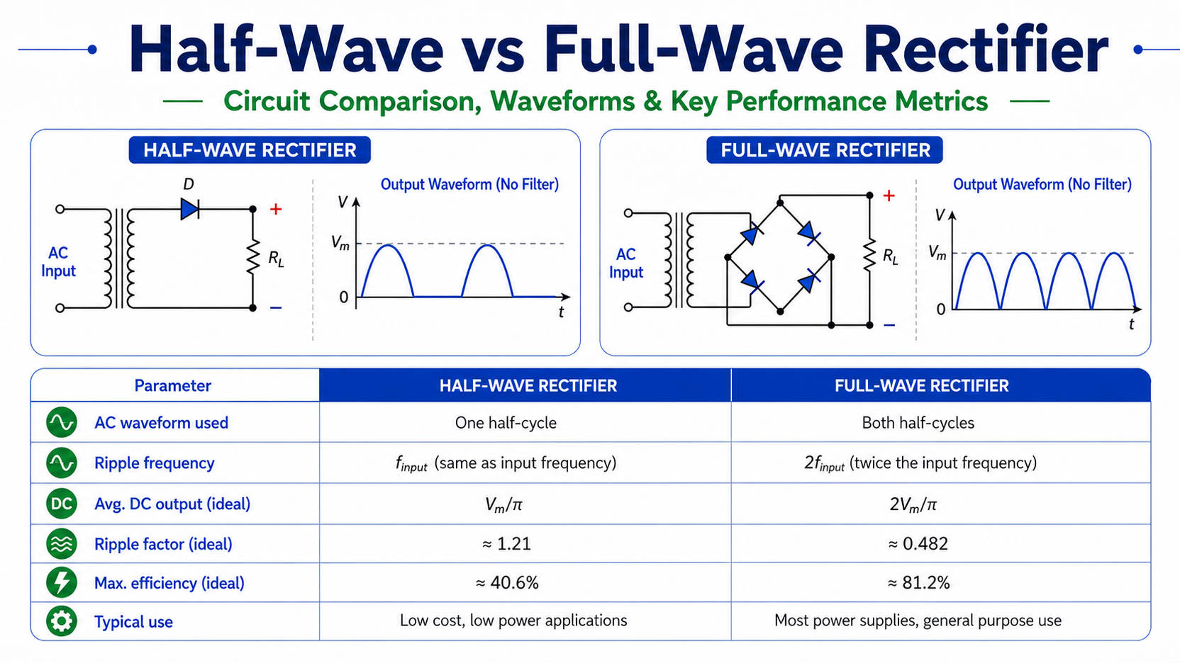
| Design factor | Half-wave rectifier | Full-wave rectifier |
|---|---|---|
| AC waveform used | One half-cycle | Both half-cycles |
| Minimum diode count | 1 | 2 center-tapped or 4 bridge |
| Ripple frequency | Equal to input frequency | Twice the input frequency |
| Ideal average output | Vm / π | 2Vm / π |
| Ideal ripple factor | About 1.21 | About 0.482 |
| Maximum ideal efficiency | About 40.6% | About 81.2% |
| Filter requirement | Larger capacitor for the same ripple | Smaller capacitor for the same load and ripple |
| Transformer utilization | Poorer | Better |
| Transformer DC bias | More likely | Better balanced |
| Typical use | Detection, bias circuits, very small loads | Power supplies, chargers, control electronics |
A half wave rectifier may be sufficient for a low-current detector, simple signal circuit, or cost-sensitive auxiliary function where ripple is acceptable. For most transformer-powered PCB inputs, full-wave rectification provides better output utilization and places less demanding requirements on the filter capacitor.
How Do You Design a Reliable Full Wave Rectifier PCB?
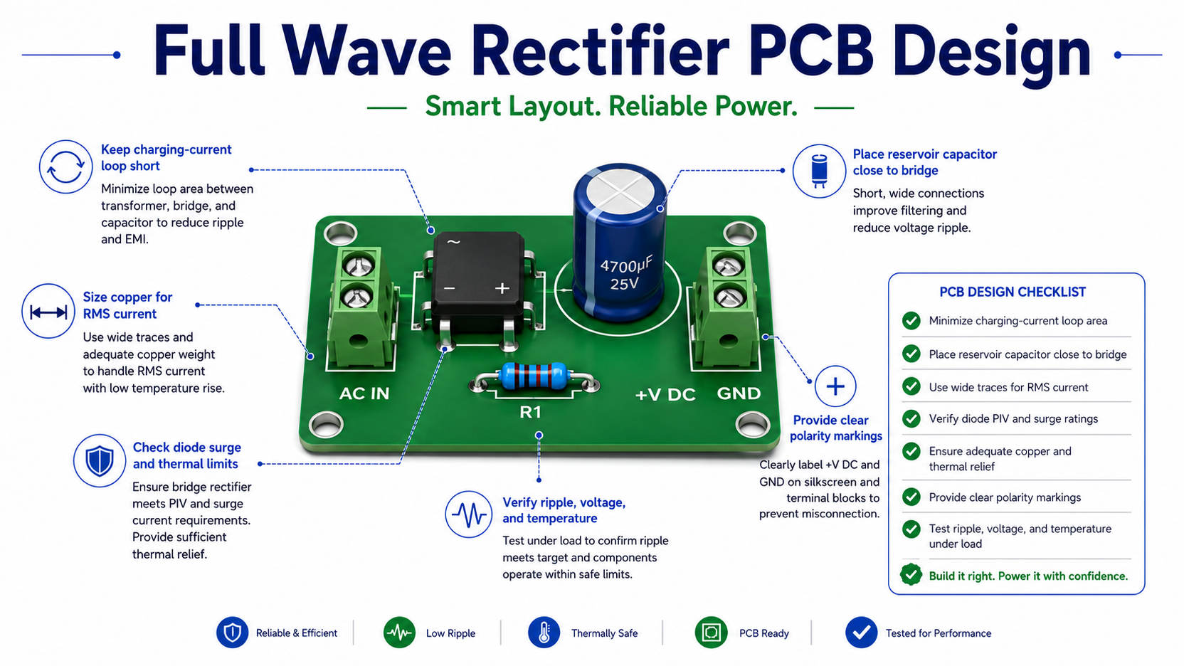
A reliable full wave rectifier PCB must be designed around peak and RMS current, not only the average DC load. With a capacitor-input filter, current flows in short charging pulses near the voltage peaks. These pulses can be several times higher than the average output current.
Select the diode from actual electrical stress
The diode or bridge should be checked for repetitive reverse voltage, average forward current, RMS forward current, repetitive peak current, non-repetitive surge current, forward-voltage loss, junction-temperature limit, package thermal resistance, and reverse-recovery behavior.
The reverse-voltage rating should include margin for transformer regulation, high-line input, switching transients, and measurement uncertainty. At 50 or 60 Hz, standard rectifier diodes are usually suitable. High-frequency transformer outputs require fast, ultrafast, or Schottky devices because reverse-recovery loss and switching noise become more significant.
Keep the charging-current loop short
The highest-current loop runs through the transformer secondary, conducting diodes, reservoir capacitor, and back to the transformer. These components should be placed close together with short, wide copper paths.
Long loops increase parasitic inductance, ringing, radiated noise, and conducted interference. Sensitive analog ground, feedback, sensing, or audio return paths should not share narrow copper with the rectifier charging current.
Size copper for pulsed current and temperature rise
Trace width should be based on RMS current, copper thickness, allowable temperature rise, ambient temperature, layer location, and enclosure airflow.
- Copper pours around bridge and diode terminals
- Thermal vias beneath suitable packages
- Wider pad necks
- Parallel copper on several layers
- Heavier copper weight where justified
- Adequate spacing from electrolytic capacitors
- Additional heatsinking for the bridge package
An integrated bridge may simplify assembly, but its junction temperature can become the limiting factor before the PCB trace reaches its current limit.
Check startup inrush and fault energy
A discharged reservoir capacitor behaves like a temporary low-impedance load. Depending on the power level, the circuit may need a fuse, fusible resistor, NTC thermistor, series resistor and bypass relay, or active inrush-limiting circuit.
The fuse must tolerate normal startup current while safely interrupting diode, capacitor, transformer, or downstream load faults. Current rating alone is not enough; time-current characteristics and interrupting capacity also matter.
Maintain suitable creepage and clearance
For hazardous-voltage circuits, conductor spacing depends on working voltage, pollution degree, overvoltage category, insulation type, material group, altitude, and the applicable safety standard.
A low-voltage full wave rectifier diagram should not be copied directly into a mains-connected PCB. Primary-side spacing, fuse placement, protective earth, connector access, isolation slots, and exposed metal parts require a product-specific safety review.
Make polarity and test points unambiguous
Silkscreen and assembly drawings should clearly identify AC input terminals, positive and negative DC outputs, diode cathodes, electrolytic capacitor polarity, fuse rating, hazardous-voltage boundaries, and voltage and ground test points.
PCB prototype validation should measure no-load DC voltage, nominal and maximum-load voltage, output ripple, startup current, diode and bridge temperature, capacitor temperature, operation at minimum and maximum AC input, and short-duration overload response. Thermal measurements should be taken after the board reaches steady-state temperature inside the intended enclosure.
AC input voltage and frequency, transformer secondary voltage and current, required DC output voltage, continuous and peak load current, maximum allowable ripple, preferred diode or bridge package, capacitor requirements, operating temperature, safety requirements, board dimensions, copper weight, Gerber files, BOM, pick-and-place data, assembly drawing, test criteria, and order quantities.
EBest Circuit can use these files to review current-loop routing, copper capacity, component spacing, polarity markings, thermal provisions, test access, and component availability before fabrication and assembly. This review is particularly valuable because the same rectifier schematic can require very different PCB construction at 0.5 A, 5 A, or 50 A.
A three-phase full wave rectifier should be treated as a separate power-design category. A typical six-pulse bridge uses six diodes and produces a higher ripple frequency, but it also introduces greater bus power, fault energy, thermal loading, and safety requirements.
FAQs
1. How many diodes are used in a full wave rectifier?
A center-tapped full wave rectifier uses two diodes, with one diode conducting during each half-cycle. A single-phase bridge rectifier uses four diodes, with two conducting at a time.
2. Is a bridge rectifier the same as a full wave rectifier?
A bridge rectifier is one type of full wave rectifier. The other common implementation is the center-tapped full wave rectifier.
3. What is the output frequency of a full wave rectifier?
The ripple frequency is twice the AC input frequency. A 50 Hz input produces 100 Hz ripple, while a 60 Hz input produces 120 Hz ripple.
4. Can a full wave rectifier produce pure DC output?
The rectifier alone produces pulsating DC. A capacitor reduces the ripple, but a regulator or additional filter stage is required for a tightly controlled DC output.
5. How do you select diodes for a full wave rectifier PCB?
Check reverse-voltage rating, average and RMS current, surge-current capability, forward-voltage loss, junction temperature, package dissipation, and recovery speed. Include margin for input tolerance, transformer regulation, capacitor inrush, load transients, and enclosure temperature.
A full wave rectifier makes use of both AC half-cycles, giving it higher average output, lower ripple, and better transformer utilization than a half wave rectifier. The bridge configuration is the usual choice for general power conversion, while a center-tapped circuit can reduce diode loss or support split supply rails.
For production hardware, reliable operation depends on more than the rectifier circuit diagram. Diode stress, capacitor ripple current, current-loop geometry, copper temperature rise, startup protection, isolation, and testing must all match the real load conditions.
For full wave rectifier PCB design review, prototyping, component sourcing, PCB assembly, or quotation support, contact EBest Circuit at sales@bestpcbs.com.
You may also like




Tags: Full Wave Rectifier, Full Wave Rectifier Circuit Diagram, Full Wave Rectifier PCB Design, Full Wave Rectifier with Capacitor Filter, Full Wave Rectifier Working