Smaller components and finer-pitch packages have changed how engineers route multilayer PCBs. A conventional through-hole structure may work well for a 0.8 mm-pitch BGA, but it often becomes restrictive once the pitch drops to 0.5 mm, 0.4 mm, or below.
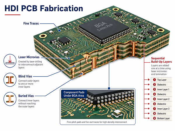
That is where HDI PCB fabrication becomes useful. A high-density interconnect PCB uses microvias, thin dielectric layers, smaller pads, and sequential lamination to create more routing channels within a limited area. It also adds laser drilling, via filling, tighter registration, and additional lamination work.
What Is HDI PCB Fabrication?
HDI PCB fabrication is the manufacture of printed circuit boards with a higher wiring density than standard multilayer boards. Common HDI features include:
- Laser-drilled microvias
- Blind and buried vias
- Fine trace and space
- Small capture pads
- Thin dielectric layers
- Via-in-pad structures
- Sequential lamination
- Stacked or staggered microvias
HDI is useful when a design must escape signals from a fine-pitch BGA, reduce board size, shorten interconnections, or increase routing density without adding an excessive number of layers.
It is often unnecessary when the PCB has enough routing space, uses larger-pitch packages, and can be completed with standard through-holes. In that case, a conventional multilayer PCB is usually more economical.
How Is an HDI PCB Different from a Conventional Multilayer PCB?
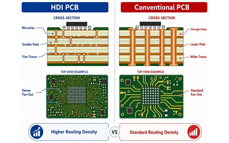
Both are multilayer PCBs, but their interconnection methods and production routes are different.
| Design factor | Conventional multilayer PCB | HDI PCB |
|---|---|---|
| Main via type | Mechanically drilled through-hole | Laser microvia, blind via, and buried via |
| Via depth | Usually passes through the complete board | Usually connects adjacent build-up layers |
| Lamination | Mainly one multilayer lamination sequence | One or more sequential build-up cycles |
| Pad size | Relatively large | Smaller capture and target pads |
| Fine-pitch BGA routing | More restricted | Better suited to dense fan-out |
| Manufacturing cost | Lower for standard layouts | Higher because of added processing |
| Main benefit | Simpler and economical | Higher routing density and smaller size |
A standard multilayer PCB remains the better option when routing can be completed without microvias. HDI becomes worthwhile when through-hole pads block routing channels or force an unnecessary increase in board size or layer count.
What Are the Main Types of HDI PCB Stackups?
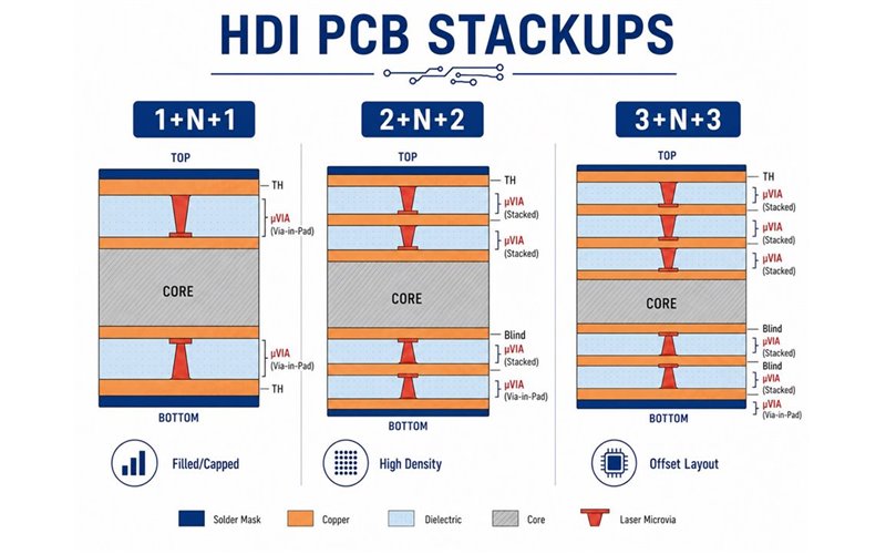
HDI stackups are commonly described as 1+N+1, 2+N+2, or 3+N+3. The outer numbers show the number of HDI build-up layers on each side. 鈥淣鈥?represents the central core structure.
| HDI stackup | Construction | Typical use |
|---|---|---|
| 1+N+1 | One build-up layer on each side | Moderate-density BGAs, industrial controls, and consumer products |
| 2+N+2 | Two build-up layers on each side | Dense processors, communication modules, and medical electronics |
| 3+N+3 | Three build-up layers on each side | Advanced computing and highly compact electronics |
| Any-layer HDI | Microvias between many adjacent layers | Highly miniaturized products and complex modules |
| Asymmetric HDI | Different build-up structures on each side | Boards with density concentrated on one surface |
A 1+N+1 construction is usually the most economical HDI entry point. Moving to 2+N+2 or 3+N+3 should be driven by actual routing needs because every additional build-up level adds process steps and registration interfaces.
What Types of Vias Are Used in High-Density Interconnect PCBs?
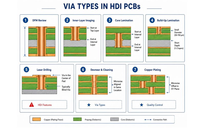
An HDI board usually combines several via types rather than using microvias everywhere.
- Plated through-hole: Connects the full board thickness and is often used for connectors, power, and component leads.
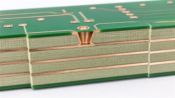
- Blind via: Connects an outer layer to one or more inner layers without passing through the complete PCB.
- Buried via: Connects internal layers and is not visible from the surface.
- Laser microvia: A small blind via used for fine-pitch routing.
- Via-in-pad microvia: Located directly inside a component pad, commonly beneath BGAs.
- Staggered microvia: Microvias on adjacent levels are laterally offset.
- Stacked microvia: Two or more microvias are aligned vertically.
- Skip microvia: Connects non-adjacent layers through more than one dielectric layer.
Large mechanically drilled vias may still be better for high current, connector strength, and thermal transfer. The via architecture should follow the electrical and routing requirements, not a desire to use the most advanced-looking structure.
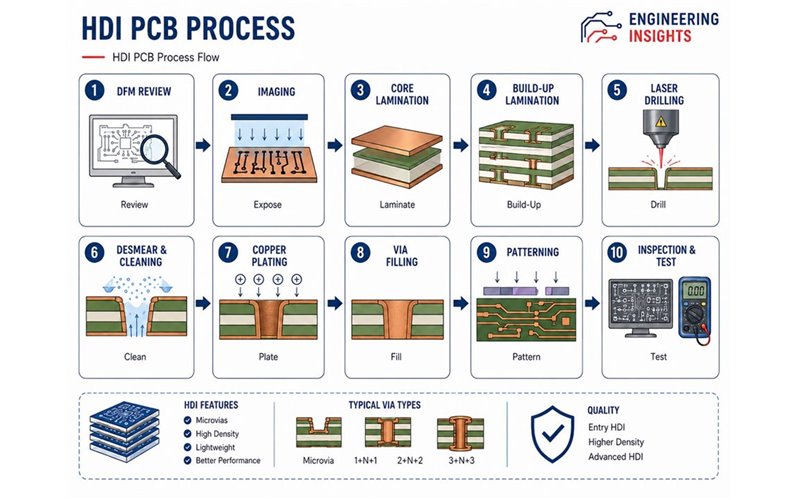
How Does the HDI PCB Manufacturing Process Work?
The exact HDI PCB manufacturing process depends on the stackup and microvia architecture. A typical route includes:
- DFM and stackup review: Confirm materials, dielectric thickness, microvia geometry, impedance, and copper weight.
- Inner-layer imaging and etching: Form and inspect the internal copper circuits.
- Buried-via processing: Drill, clean, plate, and inspect buried vias where required.
- Core lamination: Press the internal layers and prepreg into the central multilayer structure.
- Build-up lamination: Add thin dielectric and copper layers to the core.
- Laser drilling: Form controlled blind microvias.
- Desmear and cleaning: Remove laser residue and expose the target pads.
- Copper deposition and plating: Metallize the microvia walls and build the required copper thickness.
- Via filling and planarization: Fill via-in-pad and stacked microvias and level the surface.
- Repeated build-up processing: Repeat lamination, drilling, and plating for additional HDI levels.
- Final board processing: Complete through-holes, solder mask, surface finish, profiling, and legend.
- Inspection and test: Perform AOI, electrical testing, impedance testing, X-ray inspection, and microsection analysis as required.
The drill table, stackup, fabrication drawing, and layer files must show the same via start and stop layers. Conflicting data delays engineering review and can lead to an incorrect production route.
Why Is Sequential Lamination Required in HDI PCB Fabrication?
Sequential lamination is required because each microvia level is built in stages. In a 2+N+2 structure, the core is produced first, followed by the first build-up layer and its microvias. A second dielectric is then laminated over that surface before the next microvia level is drilled.
When stacked microvias are used, the lower microvia usually needs to be filled and planarized before the next microvia is placed above it.
Each additional build-up level increases:
- Lamination cycles
- Laser drilling operations
- Plating and filling work
- Registration requirements
- Thermal exposure
- Inspection requirements
- Manufacturing cost
This is why moving from 1+N+1 to 2+N+2 can affect cost and lead time more than simply adding two conventional copper layers.
What Materials Are Used for HDI PCB Manufacturing?
Material selection should consider lamination cycles, z-axis expansion, signal loss, assembly temperature, and long-term reliability.
| Material type | Suitable use | Main consideration |
|---|---|---|
| Standard FR-4 | Cost-sensitive, moderate-density HDI | May be less suitable for repeated high-temperature processing |
| High-Tg FR-4 | Industrial, automotive, and multilamination HDI | Improved thermal and dimensional stability |
| Low-CTE laminate | Reliability-sensitive microvia structures | Reduces expansion stress during thermal cycling |
| Low-loss laminate | High-speed communication and computing | Higher material and processing cost |
| Resin-coated copper | Thin build-up layers | Suitable for laser microvia formation |
| Build-up film | Very fine HDI structures | Requires specialized production capability |
| Halogen-free laminate | Products with environmental material requirements | Thermal and drilling performance must still be checked |
High-Tg FR-4 is suitable for many industrial HDI boards. A low-loss material is justified only when insertion loss, data rate, rise time, or signal-integrity targets require it.
Do not approve a laminate substitution based on Tg alone. Also compare Dk, Df, z-axis CTE, decomposition temperature, CAF resistance, moisture absorption, copper adhesion, glass style, and resin content.
HDI PCB Design Guidelines
- Confirm the stackup before routing. Dielectric thickness affects microvia depth, impedance, board thickness, and lamination.
- Use microvias only where density requires them. Standard vias can remain in open areas.
- Keep the microvia aspect ratio low. A depth-to-diameter ratio around 0.6:1 to 0.8:1 provides a wider manufacturing window.
- Use the largest practical microvia and pad. Smaller geometry increases registration and plating risk.
- Fill and cap solderable via-in-pad structures. Open vias beneath BGA pads can draw solder away from the joint.
- Limit stacked microvia levels. More stacked interfaces increase process complexity and thermal stress.
- Balance copper across the board. Uneven copper can affect resin flow, bow, twist, and plating.
- Use the production stackup for impedance calculations. Include actual dielectric thickness, copper thickness, copper profile, and solder mask.
- Keep drill definitions consistent. Every via group needs clear start and stop layers.
- Provide test coupons when needed. Impedance, registration, and microvia coupons support process verification.
A useful rule is to use the largest feature that still completes the routing. Reducing geometry simply because the CAD tool allows it reduces fabrication margin without necessarily improving the product.
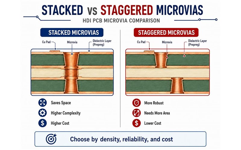
Stacked vs Staggered Microvias: Which Is Better?
Staggered microvias are usually preferred when enough lateral space is available. Stacked microvias are selected when routing density is more important than process simplicity.
| Factor | Staggered microvias | Stacked microvias |
|---|---|---|
| Routing space | Requires more lateral area | Saves board area |
| Via filling | Less demanding | Lower vias normally need complete filling |
| Registration | More forgiving | Requires tighter vertical alignment |
| Process complexity | Lower | Higher |
| Cost | Usually lower | Usually higher |
| Reliability margin | Generally wider | More dependent on interface and plating quality |
| Best fit | Industrial and reliability-sensitive products | Dense BGA escape and compact electronics |
Stacked microvias can be reliable when the lower vias are properly filled, planarized, aligned, and plated. For automotive, medical, aerospace, and long-life industrial products, staggered microvias are often the safer default unless layout density requires stacking.
What Common Defects Occur During HDI PCB Fabrication?
HDI defects are often internal, so visual inspection alone is not sufficient.
- Microvia base separation: Weak connection between plated copper and the target pad.
- Barrel or corner cracking: Related to thermal stress, copper ductility, or difficult geometry.
- Plating voids: Incomplete copper coverage inside the microvia.
- Incomplete via filling: Leaves a depression or internal void.
- Excessive dimple: Creates an uneven via-in-pad surface.
- Microvia misregistration: The drilled hole does not fully contact the target pad.
- Resin voids or delamination: Caused by contamination, inadequate resin flow, or poor lamination control.
- Fine-line opens or shorts: Linked to imaging, etching, or contamination issues.
- CAF growth: Conductive paths develop through the laminate under moisture and electrical bias.
- Bow and twist: Often related to asymmetric stackups or uneven copper distribution.
For reliability-sensitive boards, useful documentation can include microsection reports, impedance records, electrical test results, X-ray inspection, and thermal stress data.
What Factors Affect HDI PCB Fabrication Cost?
HDI cost is driven by process complexity, not only by layer count.
| Cost factor | Why it raises cost | Practical control |
|---|---|---|
| Build-up levels | More lamination and drilling cycles | Use 1+N+1 where routing permits |
| Stacked microvias | More filling, planarization, and alignment work | Use staggered vias when space allows |
| Fine trace and space | Reduces fabrication yield | Restrict fine geometry to dense areas |
| Small microvias | Tighter drilling and plating control | Use larger geometry where possible |
| Via-in-pad quantity | Adds filling and planarization | Apply only where required |
| Specialized laminate | Higher material cost and longer sourcing | Use standard high-Tg FR-4 when suitable |
| Heavy copper | Makes fine-line etching more difficult | Separate high-current and fine-routing areas |
| Quick-turn schedule | Requires priority engineering and processing | Submit complete, approved files |
| Low quantity | Setup cost is divided across fewer boards | Use a production-compatible prototype design |
| Special testing | Adds inspection and documentation | Match testing to the end-use risk |
Requesting a preliminary stackup before routing is one of the most effective cost controls. A well-planned 1+N+1 structure may replace a more expensive 2+N+2 design without affecting product performance.
Why Choose EBest Circuit for HDI PCB Fabrication?
HDI projects benefit from early communication between the customer and manufacturer. Stackup, microvia depth, filling method, material, impedance, and assembly requirements should be reviewed before final design release.
EBest Circuit, also known as Best Technology, supports HDI PCB fabrication from prototype review through PCB assembly and testing. Engineering discussions can cover:
- 1+N+1 and 2+N+2 stackup planning
- Laser microvia geometry
- Stacked and staggered via selection
- Via-in-pad filling and cap plating
- High-Tg and low-loss materials
- Controlled-impedance structures
- Fine-pitch BGA fan-out
- PCB assembly compatibility
- DFM issues affecting yield, cost, or lead time
For an accurate quotation, provide:
- Gerber, ODB++, or IPC-2581 data
- NC drill files
- Layer stackup
- Fabrication drawing
- Finished board thickness
- Copper weight
- Material requirement
- Surface finish
- Impedance table
- Via-fill requirements
- Order quantity
- Testing requirements
- Requested delivery date
FAQs
1. What does HDI mean in PCB fabrication?
HDI means high-density interconnect. It describes a PCB structure using microvias, thin dielectric layers, smaller pads, and fine routing to achieve higher wiring density.
2. What is the difference between HDI and multilayer PCB fabrication?
A conventional multilayer PCB mainly uses mechanically drilled through-holes. HDI fabrication adds laser microvias, sequential lamination, tighter registration, and often via filling.
3. What is a 1+N+1 HDI PCB?
It has one HDI build-up layer on each side of a central N-layer core. It is often the most cost-effective structure for moderate-density designs.
4. What is a 2+N+2 HDI PCB?
It has two HDI build-up layers on each side. It supports deeper microvia routing but requires more lamination and processing than 1+N+1.
5. Are HDI microvias always laser drilled?
Not by definition, but laser drilling is the standard production method because it creates small, controlled blind holes in thin dielectric layers.
6. What is the typical aspect ratio for a microvia?
A depth-to-diameter ratio of approximately 0.6:1 to 0.8:1 is commonly preferred. Ratios near 1:1 should be confirmed with the manufacturer.
7. Are stacked microvias reliable?
Yes, when they are properly filled, planarized, aligned, and plated. They still require tighter process control than staggered microvias.
8. Does via-in-pad need to be filled?
A via-in-pad beneath a soldered component pad should normally be filled and capped to prevent solder loss and provide a flat assembly surface.
9. How many lamination cycles does an HDI PCB require?
The number depends on the core, buried vias, and build-up levels. More complex structures require additional sequential lamination stages.
10. How long does quick-turn HDI PCB fabrication take?
Lead time depends on the stackup, material availability, via structure, quantity, and testing. A simple 1+N+1 prototype is normally faster than a stacked 2+N+2 or any-layer design.
11. What information should be included in an HDI fabrication drawing?
Include board dimensions, finished thickness, layer numbering, material, copper requirements, drill chart, via spans, filling requirements, surface finish, impedance values, tolerances, and inspection requirements.
12. How can engineers reduce HDI PCB manufacturing costs?
Use the simplest stackup that completes the routing. Prefer staggered microvias, standard materials, practical trace widths, and larger pads where possible. Limit via-in-pad and stacked structures to areas where they provide a measurable layout benefit.
Conclusion
HDI PCB fabrication is most valuable when fine-pitch components, limited board space, or dense routing make conventional through-hole construction impractical. The stackup, microvia structure, material, and lamination route should be settled before the layout is complete.
For an HDI stackup review, fabrication quotation, or PCB assembly discussion, contact EBest Circuit.
You may also like






Tags: HDI PCB, HDI PCB Fabrication, microvias, pcb manufacturing