





Double sided PCB boards are among the most widely used circuit board structures in electronics manufacturing. They provide conductive copper layers on both sides of an insulating substrate, allowing engineers to route more signals, place more components, and build more compact products than with a single sided PCB.
For many engineering teams, a double sided PCB board is the practical starting point for product development. It is simpler and more cost-effective than a multilayer PCB, but it gives much more routing flexibility than a one-layer board. That is why double sided printed circuit boards are commonly used in control modules, sensor boards, power interfaces, LED products, communication devices, industrial electronics, and prototype-to-production PCBA projects.
This guide explains how double sided PCB boards work, how they are manufactured, how to choose materials and surface finishes, and what to check before ordering a double sided PCB board prototype or custom production run.
What Are Double Sided PCB Boards?
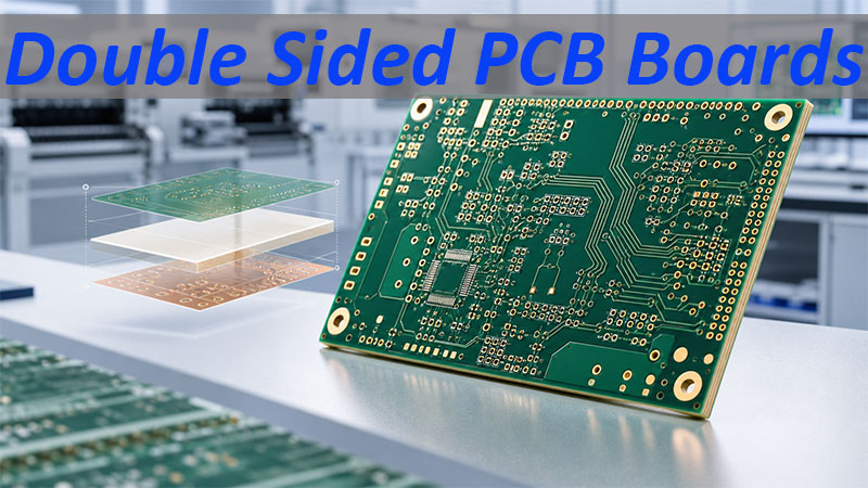
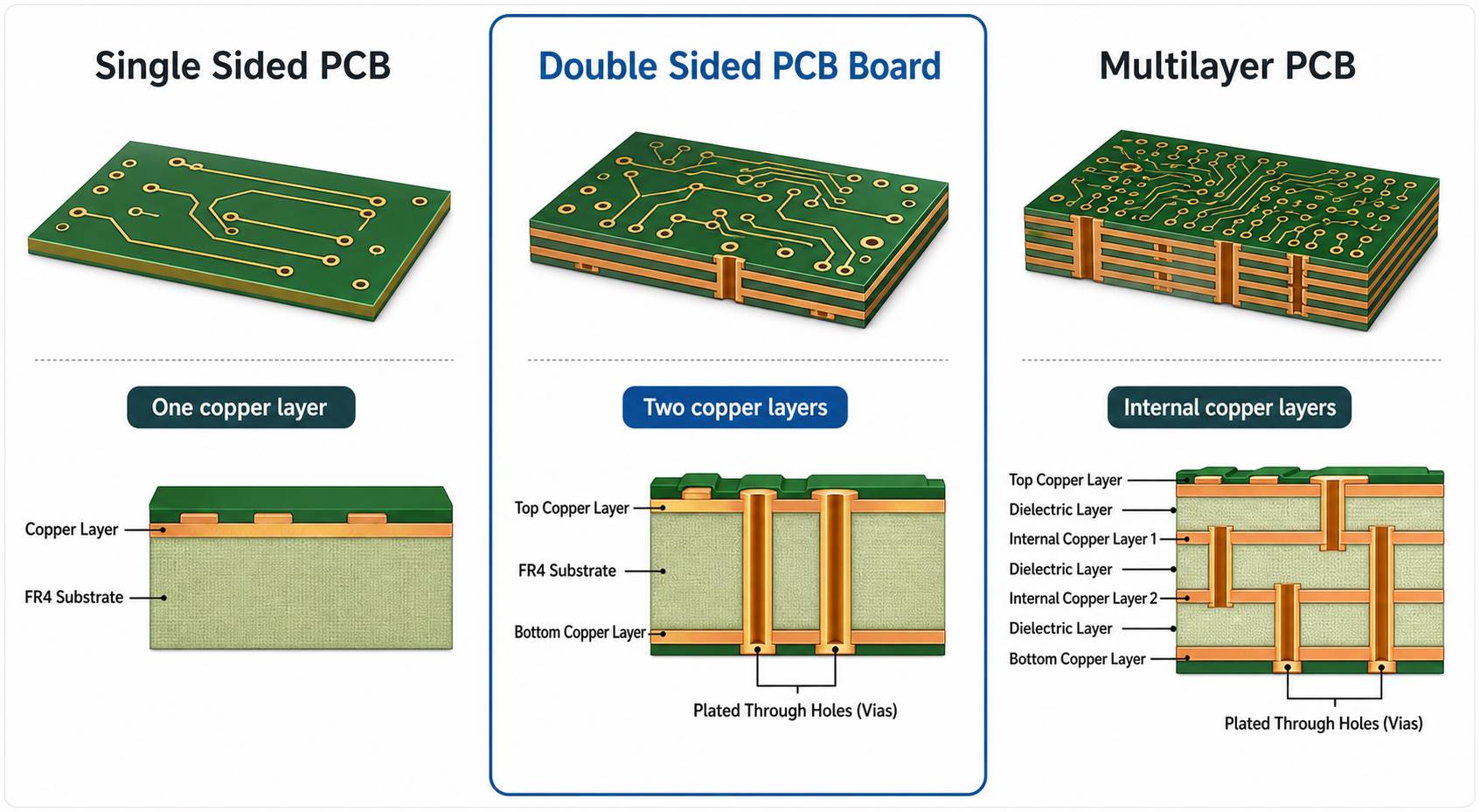
Double sided PCB boards are printed circuit boards with copper circuitry on both the top and bottom sides of the board. The two copper layers are separated by an insulating base material, usually FR4, and connected through vias or plated through holes.
In a basic single sided PCB, all routing must stay on one copper layer. This limits circuit density and can make layouts larger or less efficient. In double sided PCB boards, traces can move from one side to the other through vias. This allows signals, power, and ground paths to be arranged more efficiently.
In practical terms, double sided PCB boards are often called 2 layer PCBs. The two terms are closely related in most manufacturing and quoting situations:
| Term | Common Meaning |
|---|---|
| Double sided PCB board | A PCB with copper circuits on both sides |
| 2 layer PCB | A PCB with two conductive copper layers |
| Double sided printed circuit board | A formal name for the same PCB structure |
| Double sided copper clad PCB board | The copper-clad board structure before or during fabrication |
For engineers, the value is clear: a double sided PCB board can support denser routing, better component placement, more stable ground paths, and a more compact final assembly.
Double Sided PCB Board vs Single Sided and Multilayer PCBs
A double sided PCB board sits between a simple single sided PCB and a more complex multilayer PCB. Choosing the right structure depends on circuit complexity, product size, signal requirements, budget, and production volume.
| PCB Type | Structure | Best For | Main Limitation |
|---|---|---|---|
| Single sided PCB | Copper on one side | Simple circuits, low-cost products | Limited routing space |
| Double sided PCB board | Copper on both sides | Prototypes, control boards, compact electronics | Less routing freedom than multilayer PCBs |
| Multilayer PCB | Three or more copper layers | High-density, high-speed, impedance-controlled products | Higher cost and longer engineering review |
Single sided boards are suitable when the circuit is simple and the size is not restricted. Multilayer PCBs are better when the product needs high-speed signals, controlled impedance, complex BGA routing, or dedicated power and ground planes.
Double sided PCB boards are often the best choice when the project needs a balance between cost, routing flexibility, and manufacturability. They are especially useful in early product development because engineers can verify the circuit, test the layout, and move to small-batch production without immediately paying for a multilayer stackup.
Double Sided Copper Clad PCB Board Structure
A double sided copper clad PCB board starts with a dielectric core material laminated with copper foil on both sides. After imaging, etching, drilling, plating, solder mask, surface finishing, and testing, it becomes a finished double sided PCB board.
A typical structure includes:
- Base material, such as FR4
- Copper foil on the top side
- Copper foil on the bottom side
- Drilled holes and vias
- Plated through holes for layer-to-layer connection
- Solder mask to protect copper circuits
- Silkscreen for component marks and assembly labels
- Surface finish such as ENIG, HASL, OSP, or immersion silver
The key difference between a copper clad board and a finished PCB is processing. The copper clad laminate is the raw board material. A finished double sided PCB board has defined circuit patterns, holes, plated copper, solder mask, surface finish, and electrical testing.
For a custom double sided PCB board, engineers should pay attention to copper thickness, finished board thickness, minimum trace and spacing, minimum hole size, annular ring, solder mask bridge, and surface finish requirements. These details affect both cost and production yield.
Materials for Double Sided Printed Circuit Boards
Most double sided printed circuit boards use FR4 because it offers a practical balance of insulation, mechanical strength, cost, and availability. FR4 is suitable for many consumer electronics, industrial controls, power interfaces, test fixtures, and general electronic assemblies.
Common material and build options include:
| Item | Common Options | Why It Matters |
|---|---|---|
| Base material | FR4, high Tg FR4, aluminum, ceramic, flexible material | Determines thermal, mechanical, and electrical performance |
| Copper thickness | 0.5oz, 1oz, 2oz, or heavier copper when required | Affects current carrying capacity and trace width |
| Board thickness | Thin boards, standard 1.6mm boards, or thicker boards | Affects rigidity, assembly, enclosure fit, and mechanical strength |
| Solder mask | Green, white, black, blue, red, and other colors | Protects copper and supports inspection/branding |
| Surface finish | ENIG, HASL, lead-free HASL, OSP, immersion silver | Affects solderability, shelf life, flatness, and assembly reliability |
For SMT assembly, ENIG is often selected when the board needs a flat surface finish, good solderability, or fine-pitch component support. HASL may be suitable for cost-sensitive products with less demanding surface flatness requirements. OSP can also be used in many SMT projects, but storage and handling should be controlled carefully.
When selecting materials for double sided PCB boards, the best choice is not always the most expensive one. The right material depends on current load, operating temperature, product environment, assembly method, and expected product life.
How Double Sided PCB Boards Are Made
At EBest Circuit, a double sided PCB board order does not start directly from fabrication. It starts with engineering review. Before the board enters production, our team checks the Gerber files, drill data, stackup requirements, copper weight, board thickness, surface finish, solder mask, silkscreen, panelization notes, and any PCBA assembly files if SMT is required.
The following is a real 2 layer PCB process example from an EBest Circuit production traveler. In this case, the board used S1141 material, Tg 140, 0.865mm base thickness, H/H copper foil, and a working panel size of 260.25 x 415.00mm. The process route shows how a double sided PCB board moves from raw laminate to final shipment.
| Process Step | Control Point |
|---|---|
| Material cutting | Material, Tg, base thickness, copper foil, and panel size |
| Drilling | Drill file and minimum hole size, such as 0.95mm in this example |
| Electroless copper and panel plating | Hole copper and surface copper, such as 20um and 35um |
| Outer layer imaging | Dry film, polarity, trace width, spacing, and pad clearance |
| Outer layer inspection | Circuit pattern before plating and etching |
| Pattern tin plating | Tin plating on required circuit areas |
| Etching | Trace width, spacing, pad clearance, and line tolerance |
| Etching inspection | Visual check after circuit formation |
| Solder mask | Solder mask opening, color, and double-sided application |
| Baking | Moisture and process stability before finishing |
| Lead-free HASL | Lead-free surface finish and tin thickness, such as 1-40um |
| Flying probe test | Electrical opens and shorts |
| Profiling | Board outline and tolerance, such as +/-0.13mm |
| Final inspection | Thickness, tolerance, warpage, and IPC-A-600 standard |
| Packing | Vacuum packing, QA report, test report, samples, and humidity card |
For double sided PCB boards, drilling, copper deposition, plating, etching, solder mask, surface finish, and electrical testing are especially important. Vias and plated through holes create the electrical connection between the top and bottom copper layers. If the hole wall plating is weak, the board may pass visual inspection but fail during electrical testing, assembly, or long-term operation.
This is why EBest Circuit places DFM review before production. Our engineering team checks whether the customer’s layout is suitable for the selected process. Common review points include minimum trace and spacing, annular ring, hole size, copper-to-edge clearance, solder mask bridge, surface finish selection, finished board thickness, outline tolerance, and whether the board structure matches the assembly method.
For PCBA projects, the review also extends to BOM, component footprint, polarity, silkscreen direction, pick-and-place data, and assembly notes. This helps engineers avoid a common problem: the PCB can be fabricated, but the assembly becomes difficult or risky.
Double Sided PCB Board Prototype Cost and Lead Time
A double sided PCB board prototype is used to verify electrical function, mechanical fit, assembly feasibility, and production risk before larger-volume manufacturing. From EBest Circuit’s point of view, prototype cost and lead time are not decided by board size alone. They are decided by the full technical package.
When our team reviews a double sided PCB board prototype, we usually look at:
- Board size and panel utilization
- Board thickness
- Copper thickness
- Minimum trace and spacing
- Minimum drill size
- Surface finish
- Solder mask and silkscreen color
- Quantity
- Electrical test requirements
- SMT assembly requirements
- Component sourcing method
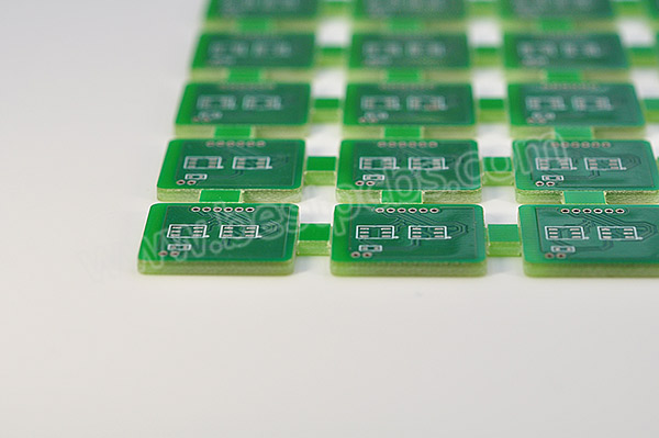
For example, one practical EBest Circuit 2L PCB project used FR4 Tg130, 1oz copper, 0.25mm board thickness, ENIG surface finish, white solder mask, and black silkscreen. The project also required SMT assembly, with components supplied by the customer.
For this type of project, the work is not only “make the bare PCB.” It becomes a coordinated PCBA prototype. The manufacturer must manage PCB fabrication, incoming material check, solder paste printing, SMT placement, reflow soldering, inspection, and final assembly review.
This is why EBest Circuit does not quote prototype timing only from the layer count. A simple bare double sided PCB board may move quickly, but a PCBA prototype also depends on component readiness, stencil preparation, assembly complexity, inspection requirements, and test scope.
For engineers, the most useful way to shorten lead time is to prepare a complete file package at the beginning: Gerber files, drill files, BOM, pick-and-place files, assembly drawing, polarity notes, and any special testing requirements. With complete files and available materials, EBest Circuit can support fast sample and small-batch PCBA delivery, with urgent PCBA projects reaching about 1.5 weeks in suitable conditions.
How to Use Double Sided PCB Board in Real Projects
Engineers use double sided PCB boards when a product needs more routing freedom than a single sided board but does not yet require a multilayer stackup. This makes them useful in many real development and production situations.
Common use cases include:
- Sensor control boards
- LED control modules
- Power interface boards
- Communication accessories
- Industrial control boards
- Consumer electronic modules
- Test fixtures
- Small embedded system boards
- Prototype boards for functional verification
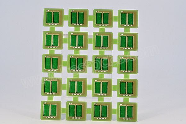
In one EBest Circuit project, the customer needed a compact 2 layer PCB with SMT assembly. The board used FR4 Tg130, 1oz copper, 0.25mm finished thickness, ENIG surface finish, white solder mask, and black silkscreen. The customer supplied the components, while EBest Circuit supported PCB fabrication and SMT assembly.
This is a good example of how double sided PCB boards are used in real product development. The board was thin, so mechanical handling and assembly support had to be considered. ENIG was selected to provide a flat soldering surface for SMT. The white solder mask and black silkscreen helped with visual identification, assembly marks, and product appearance.
In this type of 2 layer PCB layout, the top layer may carry key components and signals, while the bottom layer may support additional routing, ground return paths, and connector placement. With proper via planning, the layout can stay compact without moving immediately to a 4 layer PCB.
For PCBA projects, a double sided PCB board may also support components on one side or both sides. If components are placed on both sides, the assembly process must consider soldering sequence, component weight, reflow profile, inspection access, and whether any parts require hand soldering or selective soldering.
This is where practical engineering support matters. A manufacturer that understands both PCB fabrication and PCB assembly can help identify layout and assembly risks before production, not after boards are already made. At EBest Circuit, one business contact works together with three engineering support roles to respond to engineering needs across DFM review, BOM optimization, PCB manufacturing, SMT assembly, and testing.
Custom Double Sided PCB Board Layout Guidelines
A custom double sided PCB board should be designed with manufacturing and assembly in mind. Here, layout does not mean full circuit design or schematic development. It means the practical PCB layout and DFM decisions that help the board move smoothly into fabrication and assembly.
Important layout guidelines include:
- Keep trace width and spacing within the manufacturer capability.
- Use proper annular ring around vias and plated holes.
- Avoid placing vias too close to pads unless via-in-pad is intentionally specified.
- Maintain sufficient solder mask bridge between fine-pitch pads.
- Keep copper balance reasonable on both sides of the board.
- Use clear polarity and orientation marks for SMT assembly.
- Confirm connector placement and mechanical clearance.
- Provide complete Gerber, drill, BOM, pick-and-place, and assembly files for PCBA.
- Use test points where functional testing is required.
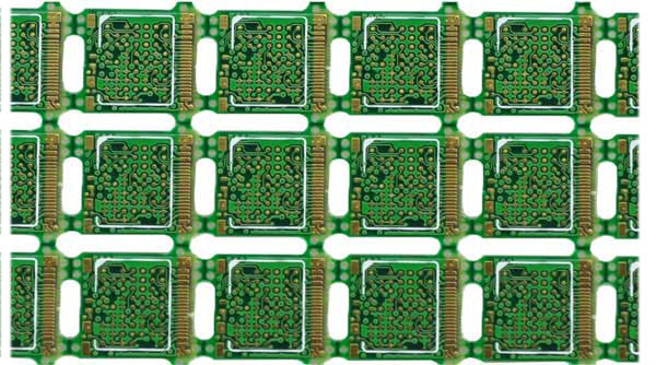
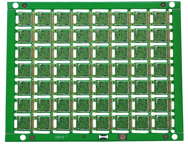
- Review panelization requirements before production.
For 1oz copper double sided PCB boards, trace width and spacing should be selected based on current, voltage, impedance needs, and the factory’s production capability. A layout that looks correct on screen may still create fabrication risk if it pushes minimum spacing, drill, or solder mask limits too aggressively.
EBest Circuit provides DFM analysis and process adaptation suggestions through an engineering support team with long-term PCB and PCBA experience. For engineers, this helps reduce repeated revisions, avoid unclear fabrication notes, and improve the chance of successful first-run production.
When to Choose a Double Sided Flexible PCB Board
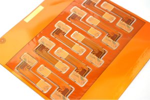
A double sided flexible PCB board is different from a standard rigid FR4 double sided PCB board. It uses flexible base material and is designed for products that require bending, folding, or space-saving interconnection.
Double sided flexible PCB boards may be suitable for:
- Wearable electronics
- Compact medical devices
- Display modules
- Camera modules
- Sensor connections
- Foldable or moving electronic assemblies
- Space-limited product designs
However, flexible PCBs require different design and manufacturing rules. Bend radius, coverlay openings, stiffener placement, copper type, dynamic bending requirements, and connector reinforcement all need attention. A layout that works on rigid FR4 may not be suitable for a flexible circuit.
If the product only needs a compact but rigid assembly, a standard double sided PCB board may be more cost-effective. If the product needs repeated bending or tight mechanical integration, a double sided flexible PCB board or rigid-flex PCB may be the better option.
Why Work with a Double Sided PCB Boards Manufacturer with PCBA Support
Choosing a double sided PCB boards manufacturer is not only about bare board price. For engineering teams, the real value often comes from file review, manufacturability feedback, component support, assembly control, testing, traceability, and delivery management.
EBest Circuit (Best Technology), founded in 2006, provides customized PCB and PCBA solutions for global customers. The service scope includes FR4 PCB, metal core PCB, ceramic PCB, special PCB, PCB prototype, mass production, component sourcing, and PCB assembly.
For double sided PCB boards and 2 layer PCB projects, the company can support:
- PCB fabrication
- Component sourcing
- Customer-supplied component assembly
- SMT assembly
- PCBA testing
- Prototype and small-batch production
- DFM pre-review
- BOM optimization suggestions
- Engineering process adaptation advice
The company operates its own PCB and PCBA factory, works with more than 1,000 supply chain partners, and has served more than 10,000 engineers and over 1,800 customers. Its quality system includes ISO 9001, ISO 13485, IATF 16949, AS9100D, REACH, RoHS, and UL-related compliance support.
For production traceability, a digital workshop can track materials, product batches, production cycle, and production progress quickly. This helps engineering teams manage quality, schedule, and repeat orders more clearly.
The best result comes when engineers and manufacturers work together early. If the PCB manufacturer reviews the Gerber files, BOM, assembly notes, and process requirements before fabrication, the project has a better chance of moving from prototype to production without costly delays.
FAQs about Double Sided PCB Boards
What are double sided PCB boards?
Double sided PCB boards are printed circuit boards with copper circuits on both the top and bottom sides. The two layers are connected by vias or plated through holes, allowing more compact and flexible routing than a single sided PCB.
Is a double sided PCB board the same as a 2 layer PCB?
In most manufacturing and quoting contexts, yes. A double sided PCB board usually means a 2 layer PCB with one copper layer on each side of the board.
What is a double sided copper clad PCB board?
A double sided copper clad PCB board is the base board material with copper foil laminated on both sides. After imaging, etching, drilling, plating, solder mask, surface finish, and testing, it becomes a finished double sided PCB board.
When should I use a double sided PCB board?
Use a double sided PCB board when a single sided board cannot provide enough routing space, but the project does not need the cost or complexity of a multilayer PCB. It is a practical choice for many prototypes, control boards, and compact electronic products.
What affects double sided PCB board prototype cost?
Prototype cost depends on board size, thickness, copper weight, surface finish, trace and spacing requirements, drill size, quantity, electrical testing, and whether SMT assembly or component sourcing is required.
Can double sided PCB boards support SMT assembly?
Yes. Double sided PCB boards are widely used for SMT assembly. For PCBA projects, engineers should provide Gerber files, BOM, pick-and-place files, assembly drawings, and any special testing requirements.
What files are needed for a custom double sided PCB board?
Most projects require Gerber files, drill files, board specifications, solder mask and silkscreen requirements, and surface finish selection. PCBA projects also require BOM, pick-and-place files, assembly notes, and test requirements.
What is the difference between a double sided PCB board and a double sided flexible PCB board?
A standard double sided PCB board is usually rigid, often made from FR4. A double sided flexible PCB board uses flexible material and is designed for bending, folding, or compact interconnection in space-limited products.
How can DFM review help double sided PCB boards?
DFM review checks whether the board can be manufactured reliably. It can identify risks such as insufficient spacing, small annular rings, unclear drill data, solder mask issues, panelization problems, and assembly mismatches before production starts.
How do I choose a double sided PCB boards manufacturer?
Choose a manufacturer that can support PCB fabrication, engineering review, material selection, SMT assembly, testing, quality control, and delivery management. For prototype and PCBA projects, one-stop support can reduce communication gaps and production risk.
Ready to Build Your Double Sided PCB Boards?
If you are working on a double sided PCB board prototype, a 2 layer PCB layout, or a PCBA project that needs fabrication, components, SMT assembly, and testing, you do not have to solve every production detail alone.
Send your Gerber files, BOM, pick-and-place file, drawings, or even early project questions to EBest Circuit. Our team will review the details carefully and help you find a practical way forward.
Email us at sales@bestpcbs.com. Tell us what you are building, what stage you are in, and what worries you most. We will help you turn the board from a file on your screen into a working product in your hands.
You may also like


Tags: Double Sided Copper Clad PCB Board, double sided pcb board prototype, Double Sided PCB Boards