

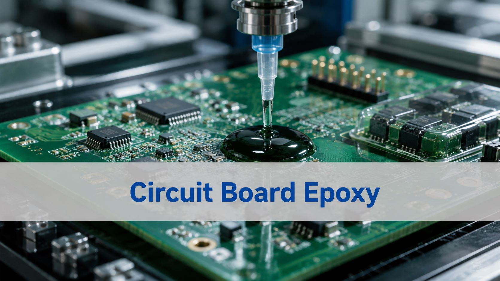
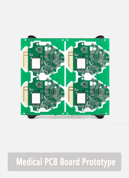
Circuit board epoxy is a high-performance thermosetting polymer matrix utilized as a structural substrate layer, a protective coating, or an encapsulation compound to isolate copper tracks and electronic components from external hazards. This industrial-grade resin plays a critical role in electronics manufacturing by providing exceptional dielectric strength, mechanical reinforcement, and defense against harsh operating environments. This technical guide explores how circuit board epoxy is applied across the PCB fabrication and PCBA (Printed Circuit Board Assembly) phases to maximize product lifespans and safeguard intellectual property.
What is Circuit Board Epoxy and Its Critical Role in PCB Assembly?
When looking at a completed electronic module, engineers often wonder: why is there epoxy on circuit boards in the first place? At its core, circuit board epoxy resin is a thermosetting polymer that transitions from a liquid state into an incredibly tough, chemically inert solid layer. During the turnkey assembly process, applying specialized epoxy for circuit board protection serves three critical engineering purposes:
- Mechanical Reinforcement: It anchors heavy components against high-vibration environments.
- Electrical Insulation: It provides high dielectric strength, preventing high-voltage arcing between closely spaced traces.
- Environmental Isolation: It blocks moisture, salt spray, and corrosive chemicals from reaching copper layers and solder joints.
For modern printed circuit board epoxy applications, choosing the right formulation ensures that your layout performs reliably under real-world operating conditions without degrading signal integrity.
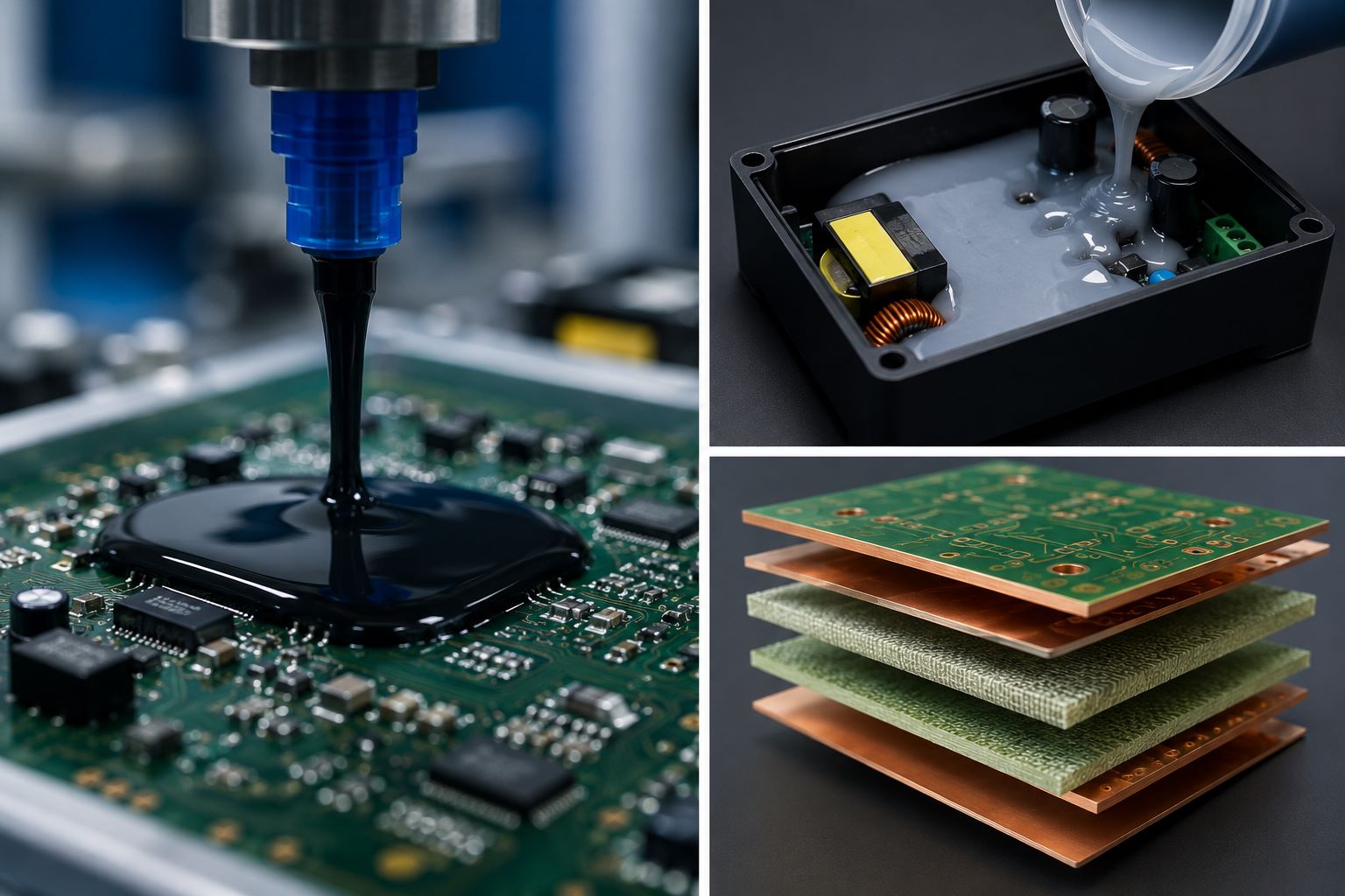
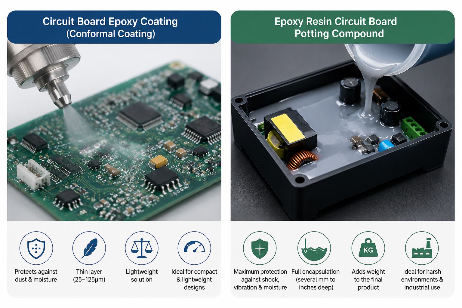
Circuit Board Epoxy Coating vs. Potting Compound in PCBA Services
When configuring post-assembly protection in a PCBA workflow, electronic manufacturing services (EMS) providers generally deploy two primary methods: conformal coating and encapsulation.
| Feature | Circuit Board Epoxy Coating | Epoxy Resin Circuit Board Potting Compound |
| Application Process | Spraying, brushing, or selective automated dispensing. | Complete submersion within a housing or mold cavity. |
| Thickness | Typically 25 μm to 125 μm. | Several millimeters to inches deep. |
| Mechanical Defense | Moderate (protects against dust and light moisture). | Extreme (absorbs severe shock, impact, and deep vibration). |
| Weight Impact | Minimal added weight. | Significant weight addition to the final enclosure. |
While an epoxy coating of circuit boards is ideal for precision weight-saving enclosures, an epoxy resin circuit board potting compound is the preferred choice for heavy-duty industrial applications where components must be completely sealed off from the elements. Additionally, specialized high-viscosity epoxy to hold down circuit boards can be dispensed locally on heavy components like transformers or large capacitors before the full encapsulation process begins.
Methods of Conformal Coating Application in PCBA Production
When establishing an optimal protective barrier, implementing a professional conformal coating circuit board process requires selecting a method that matches the assembly’s volume and geometry. In modern electronics manufacturing, there are three primary industrial techniques used to explain how to apply conformal coating to pcb modules:
- Automated Selective Coating: For high-reliability and high-volume runs, our facility utilizes automated selective coating pcba systems. Controlled by multi-axis robotic dispensers, these machines precisely apply the coating layer with micron-level repeatability. This process completely eliminates human error, ensuring consistent edge definition and thickness without overlapping onto critical exclusion areas.
- Manual Spraying: Ideal for small-batch prototypes or highly complex assemblies with vertical components. Technicians use professional spray guns inside dedicated ventilation hoods, maintaining a uniform film thickness (25μm to 125μm) across the target areas.
- Dipping (Immersion): The assembly is mechanically submerged into a coating vat at a controlled rate, guaranteeing 100% coverage underneath low-profile components. This method is highly effective for ruggedized hardware that doesn’t feature sensitive, unsealed parts.
DFM Standards: Which Components Must NOT Be Conformal Coated
A fundamental pillar of our manufacturing process control is establishing strict pcb keep out areas for conformal coating. While these chemical resins excel at blocking moisture and dust, applying them to the wrong areas can insulate electrical contacts, alter mechanical tolerances, or trap gases, resulting in catastrophic field failures.
When conducting a DFM review, our engineers identify what components cannot be coated on a pcb:
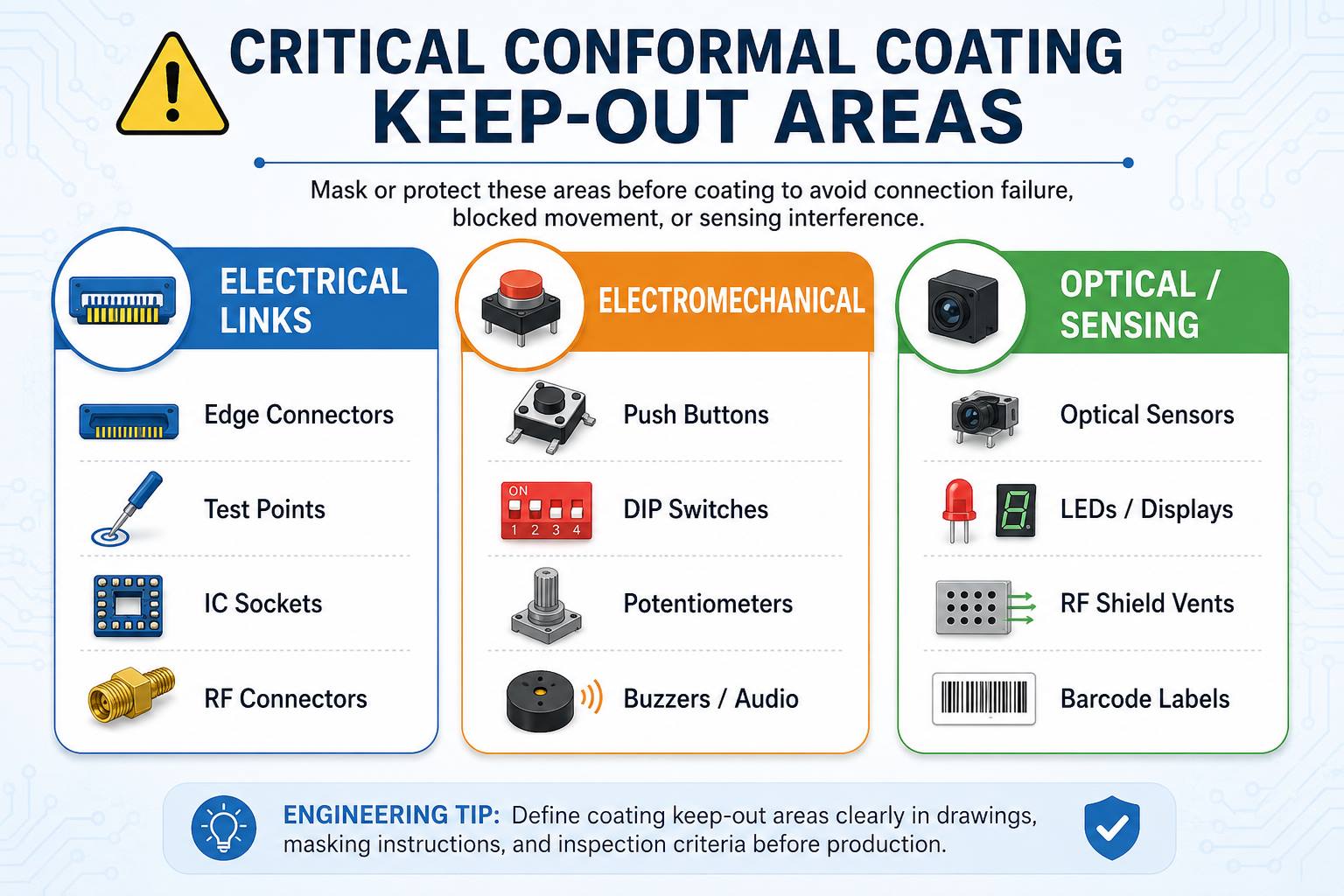
To safeguard these sensitive keeping-out areas, we deploy a rigorous conformal coating masking process before the assembly reaches the coating line. Our production technicians use specialized, residue-free polyimide masking tapes, custom silicon boots, or peelable liquid masks to temporarily seal off vulnerable pins and housings.
Once the curing oven cycle concludes, this masking material is meticulously peeled away under ESD-safe conditions, leaving clean, pristine copper pads ready for final housing integration and rigorous functional testing.
Engineering Insight: Materials Matter in Glass Epoxy Circuit Boards (FR4)
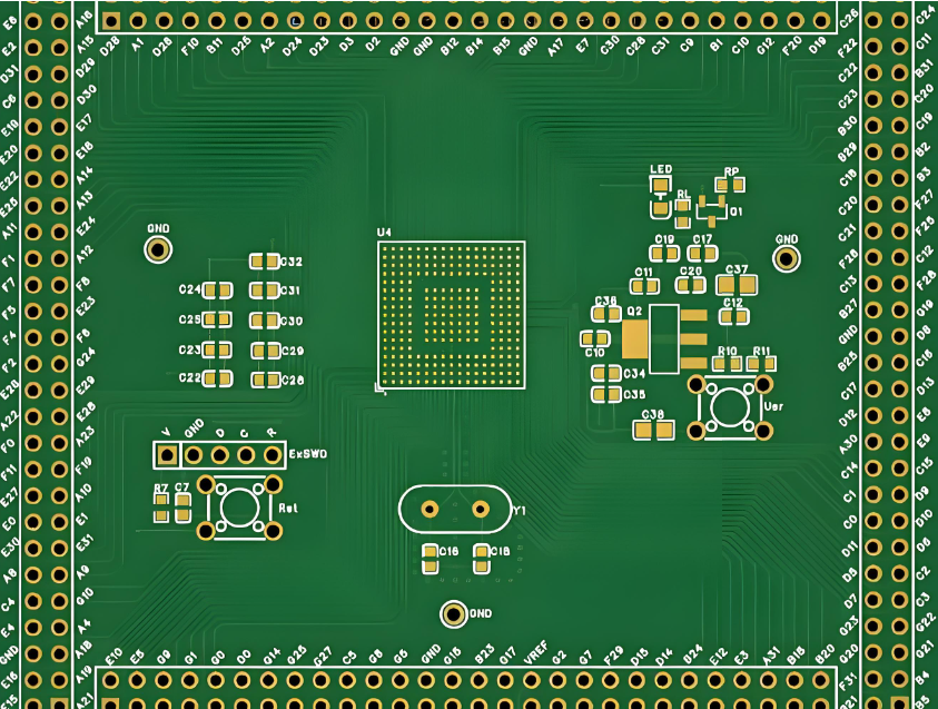
The relationship between epoxies and PCBs begins long before the assembly line. In base substrate manufacturing, the most ubiquitous material in the industry is FR4.
The common name for epoxy fiberglass circuit boards is FR4 (Flame Retardant 4). This structural foundation is a glass epoxy circuit board material constructed by impregnating woven fiberglass mats with a flame-retardant epoxy resin matrix under intense heat and pressure.
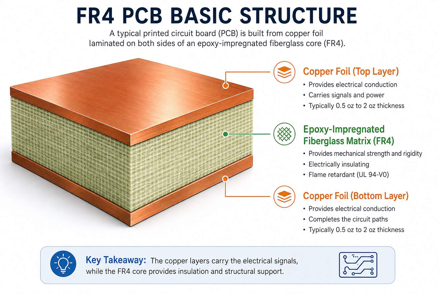
When specifying a printed circuit board sheets fr4 material fiberglass epoxy sheet, layout designers must carefully consider the resin’s glass transition temperature (Tg) and Coefficient of Thermal Expansion (CTE). Matching these thermal properties ensures that the fr4 epoxy circuit board retains its structural rigidity and doesn’t delaminate during multi-stage reflow soldering or automated wave soldering operations.
Understanding Black Epoxy on Circuit Boards: IP Protection and Durability
It is common to find sections of high-end consumer electronics or industrial controllers obscured by an opaque, dark layer. Utilizing black epoxy on circuit board assemblies serves a dual purpose for product developers.
First, from an engineering perspective, a circuit board black epoxy provides excellent thermal dissipation and hides surface imperfections. Second, and perhaps more importantly for B2B OEMs, it provides robust intellectual property (IP) protection.
Why is black epoxy put on circuit boards? > By completely covering proprietary chipsets, specialized layout architectures, and custom microcontrollers with an opaque block of resin, it prevents competitors from performing visual reverse-engineering or tracing circuit paths without destroying the underlying silicon.
DFM Guide: How We Evaluate Epoxy Resin for High-Reliability PCB Potting
From a Design for Manufacturing (DFM) standpoint, a one-size-fits-all approach to chemical protection does not exist. A common misconception among procurement managers is asking: will any epoxy work as circuit board potting? The short answer is no. Utilizing consumer-grade epoxies can lead to catastrophic field failures due to exothermic shrinkage, high moisture absorption, or trace corrosion from aggressive curing agents. When a manufacturing partner evaluates an epoxy resin circuit board potting requirement for a custom layout, our engineering teams look closely at three main metrics to identify the best epoxy for circuit boards:
- Thermal Conductivity: High-power density boards require filled epoxies that pull heat away from active switching components (like MOSFETs) to external heat sinks.
- Cure Shrinkage Rate: Low-shrinkage formulations prevent stress fractures on delicate surface-mount device (SMD) solder joints during the cross-linking process.
- Chemical Composition: Acid-free, neutral-cure formulas (such as two-part addition-cure systems) are strictly mandated to prevent chemical corrosion of copper structures.
Reworking and Replacing Components: How Technicians Handle Cured Epoxy Safely
While epoxy provides unparalleled environmental resilience, it introduces challenges when a product requires an engineering change order (ECO) or component swap during prototype evaluation. Because industrial resins are designed to be permanent, figuring out how to remove epoxy from circuit board assemblies requires precision engineering controls.
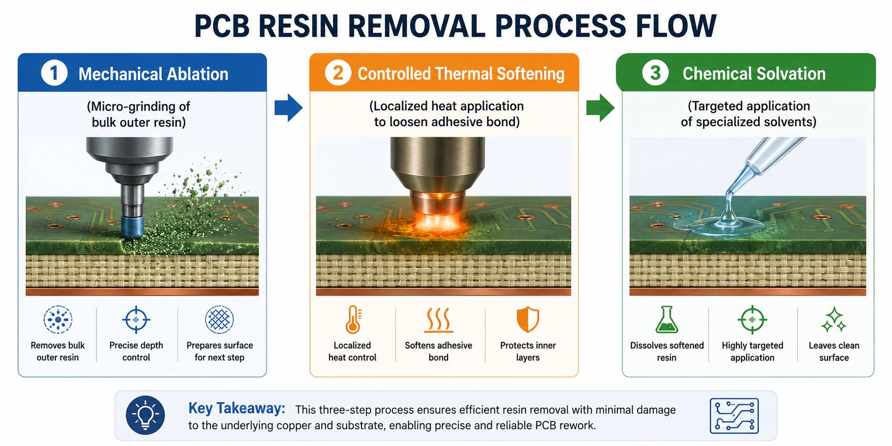
To safely remove epoxy from circuit board real estate without destroying surrounding multi-layer copper tracks, technicians use localized thermal softening combined with micro-abrasion tools. For dense areas, a targeted application of specialized chemical stripping agents breaks down the cross-linked polymer.
This controlled process ensures that any necessary circuit board black epoxy removal is executed cleanly, leaving the delicate laminate intact for pad restoration and component replacement.
Maximizing PCB Performance: High Temperature and Weatherproof Sealing Solutions
For electronics destined for subsea deployment, aerospace systems, or high-temperature downhole drilling, standard coatings fall short. Advanced assemblies require a ruggedized, waterproof circuit board epoxy matrix designed to handle intense environmental changes.
Implementing a high temperature epoxy for circuit boards enables continuous operation in environments exceeding 150 Degrees Celsius without experiencing material outgassing or dielectric breakdown. Furthermore, a precision-applied seal protects vulnerable surface tracks from prolonged exposure to humidity, salt atmospheres, and sudden thermal cycling. This ensures the underlying electronics maintain strict performance parameters over decades of operation.
Advanced PCBA: Multilayer Circuit Boards and Epoxy Via Filling Technologies
As layouts compress and signal speeds climb, epoxies move inside the board itself. In complex, high-density multilayer circuit boards epoxy resin formulations serve a highly specialized electrical role: via-in-pad plugging.
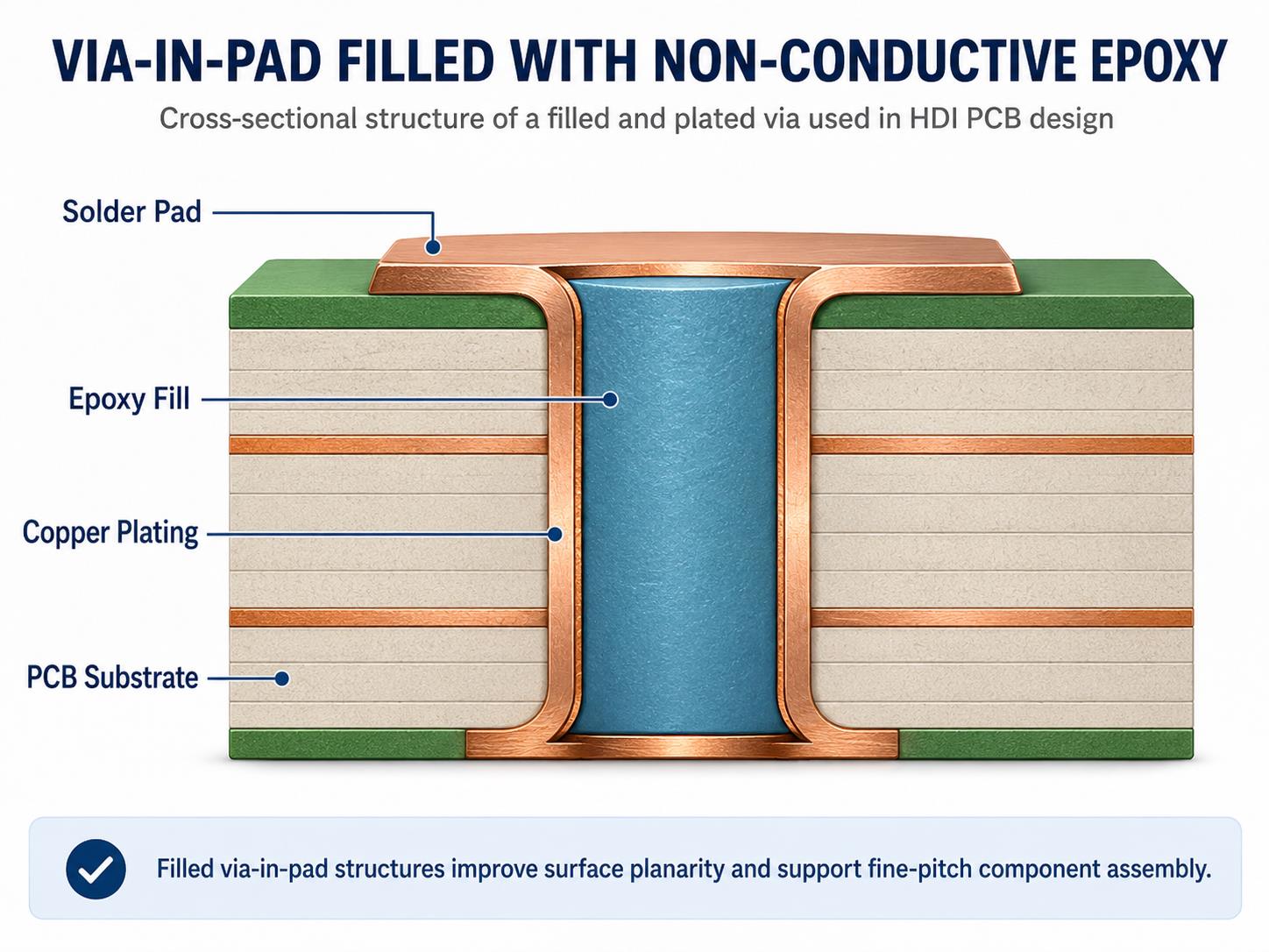
When building High-Density Interconnect (HDI) boards, standard open vias can cause solder migration away from the SMD pads during reflow. To prevent this, fabricators use materials like the industry-standard mazz epoxy hole filler printed circuit board compound to plug the microscopic microvias.
Once the via is plugged with a non-conductive or printed circuit board epoxy fill conductive paste, the surface is planarized and plated over with copper (known as POVR – Pad Over Via Resin). This advanced technology allows hardware designers to place vias directly underneath fine-pitch BGA components, maximizing routing space while preserving signal integrity.
Quality Control Standards for Epoxy Application in One-Stop PCBA Services
Executing a flawless epoxy application or potting cycle requires rigorous process control. Without strict oversight, common defects like air entrapment, incomplete curing, or internal voids can form inside the assembly.
To combat this, an elite manufacturing workflow utilizes a dedicated cross-functional engineering framework. Every project is assigned an experienced account manager paired with a specialized triad of engineers—covering layout optimization, fabrication DFM, and automated assembly diagnostics.
This engineering team carefully manages the entire thermal profile of the epoxy application:
- Vacuum De-airing: Eliminating microscopic bubbles from potting mixtures prior to dispensing.
- Precision Pre-Baking: Eliminating moisture from the FR4 substrate to prevent internal delamination.
- Controlled Cure Ovens: Following strict ramp-up and cool-down temperature curves to minimize structural stress on delicate internal board layers.
Why Partner with EBest for Advanced Circuit Board Epoxy Applications and Turnkey PCBA?
At EBest, we understand that mastering circuit board epoxy chemistry is only the first step toward delivering zero-defect electronics. Achieving true hardware reliability at scale requires an integrated manufacturing partner. Here is how EBest transforms your technical requirements into high-performance, market-ready products:
- Expert 1+3 Technical Support Model: For every project, you are assigned one dedicated account manager and three specialist engineers (spanning PCB layout, DFM fabrication, and PCBA assembly control) to collaboratively review your files and optimize your epoxy profiles.
- Automated Selective Precision: Our facility utilizes advanced automated multi-axis robotic dispensing systems, ensuring uniform thickness for circuit board epoxy coating and potting without risking overflow onto critical exclusion zones.
- Robust IP Defense & Ruggedization: We offer specialized circuit board black epoxy encapsulation and high-temperature (150 ℃) material processing to shield your proprietary layouts from both environmental hazards and reverse-engineering.
- Seamless Turnkey Execution: From multi-layer FR4 glass epoxy substrate fabrication and precise components sourcing to advanced via filling and final product assembly, we manage your entire production lifecycle under one roof.
Ready to ruggedize your next electronic assembly? A warm welcome to contact EBest anytime via email at sales@bestpcbs.com to upload your BOM and Gerber files, and experience our high-speed, professional turnkey engineering services.
FAQs About Circuit Board Epoxy in PCB Manufacturing
Q1: Can bubbles in epoxy on a circuit board cause problems during assembly?
Yes. Trapped air bubbles create internal voids. Under high voltage, these voids can cause localized corona discharges and high-voltage arcing, leading to insulation breakdown. In high-power modules, air pockets act as thermal barriers, trapping heat and causing components to burn out prematurely.
Q2: Is printed circuit board epoxy fill always conductive?
No. Fabricators utilize both conductive (silver-filled) and non-conductive epoxies. Non-conductive epoxy filling is far more common for standard via-in-pad structures because it matches the thermal expansion properties of the surrounding FR4 laminate more closely, reducing thermal stress fractures.
Q3: How do manufacturers cure conductive epoxy properly?
Conductive and structural epoxies require a precise thermal profile inside automated industrial curing ovens. Technicians carefully control the temperature ramp rate to ensure uniform cross-linking across the entire surface area, preventing internal mechanical stresses that could warp thin multilayer substrates.
Q4: Do you provide standalone electronic repair services for potted boards?
No. As an industrial-grade PCB manufacturing and PCBA processing facility, we do not provide standalone consumer repair services for third-party electronics. We do, however, provide comprehensive engineering rework and design modifications for batch production orders and prototype series handled directly inside our manufacturing facility.
You may also like


Tags: circuit board epoxy, conformal coating, PCB Protection Materials