

Wondering if thermal stress test for PCB is to ensuring long-term board stability? This practical guide covers core definitions, operational steps, official standards, common flaws, testing parameters, and required equipment to help you avoid practical application failures. It’s a valuable resource to help you protect against costly field failures and product recalls that are entirely preventable.
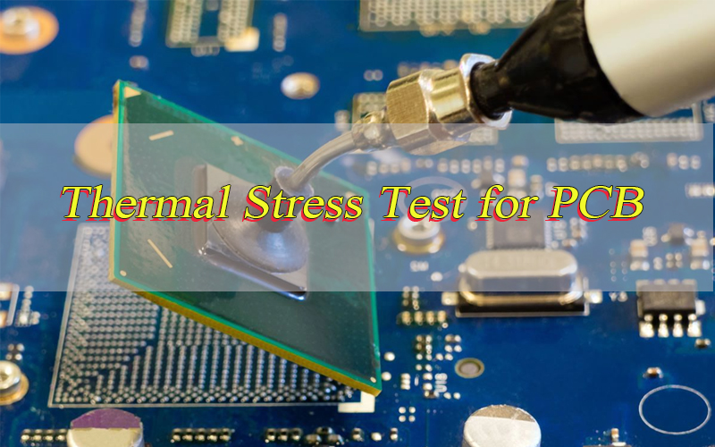
What is a Thermal Stress Test for PCB?
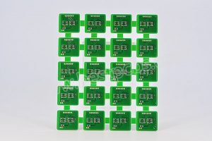
A thermal stress test for PCB aims to check the actual bearing capacity of finished printed circuit boardsprinted circuit boards against regular temperature changes. Thermal stress tested for PCB can expose hidden structural weak points that ordinary electrical performance checks cannot find, and these hidden issues will gradually trigger equipment breakdowns in actual working scenes.
Different raw materials used in PCB production such as copper foil insulating base material and protective solder mask all feature distinct expansion and shrinkage degrees when temperature rises or drops. Long term temperature changes will generate strong shear force on the joint positions of different materials including inner board connecting holes and surface welding areas. The whole set of thermal stress test for PCB work adopts controllable repeated temperature change modes to speed up the appearance of such structural damages, so production teams can finish quality confirmation before formal mass production.
Why Do Thermal Stress Test for PCB?
Carrying out complete PCB thermal stress testing helps all kinds of circuit board products keep stable mechanical structure and normal electrical functions under different working temperature environments. Most unstable working faults of high standard electronic products come from fatigue damage caused by long term temperature changes instead of simple production flaws.
- Cut down on on site operational faults: Frequent temperature shifts will bring about inner layer separation circuit copper layer falling off and circuit disconnection, which will directly lead to product maintenance troubles and hidden safety risks.
- Verify rationality of raw material selection: Common base materials including standard FR 4 high temperature resistant FR 4 and polyimide show different resistance to temperature related stress. Relevant testing work can confirm whether selected materials match the actual working temperature range.
- Check overall production processing quality: Substandard pressing work insufficient copper layer adhesion strength and irregular welding operation will leave many fragile positions on boards, all of which can be fully found via thermal stress test for PCB.
- Meet unified industrial access rules: Electronic products used in vehicle equipment medical treatment and industrial control fields all need to pass relevant thermal resistance verification to meet unified long term stable operation requirements.
- Control overall project running costs: Finding out unqualified products in the sample testing stage can avoid large scale design revisions product recalls and follow up after sales maintenance expenditure in the later period.
How is Thermal Stress Tested for PCB?
All standard thermal stress tested for PCB operations follow fixed practical steps to restore real ambient temperature changes, meanwhile keeping consistent testing conditions to ensure comparison results stay accurate and effective.
- Complete sample sorting work: Pick out intact PCB finished products that conform to actual production standards, record detailed data including adopted raw materials total board layers and surface processing types, and wipe away surface stains that may interfere with final detection results.
- Finish basic visual and electrical pre inspection: Check board surfaces for obvious scratches deformation and early layering problems. Conduct circuit conduction detection and insulation performance testing to record the initial working state of tested samples.
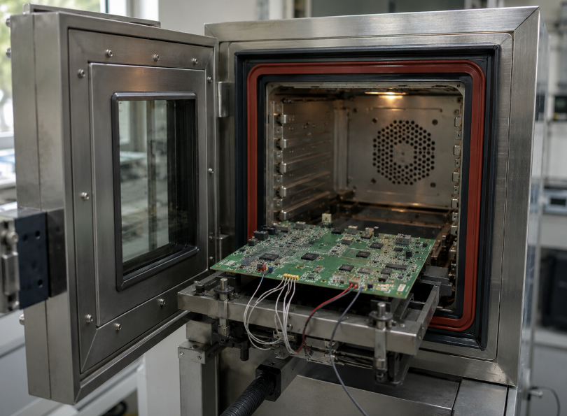
- Place samples inside professional testing equipment: Put sorted PCB samples steadily into temperature cycling testing cabinets, leave enough flowing space between every single board, and avoid direct contact between samples to prevent uneven heating and cooling situations.
- Set matched temperature running curves: Input accurate testing data according to industrial unified rules or actual product usage demands. The widely adopted temperature range covers -40°C to +125°C, with stable standing time set as 30 minutes at both highest and lowest temperature points.
- Start formal cyclic temperature changing work: Turn on the testing device to run repeated temperature adjustment processes. Most industrial verification projects need to finish 100 to 500 complete cycles according to different product application scenes.
- Carry out regular midway condition checks: Take out testing samples after finishing every 50 to 100 temperature cycles, redo surface observation and electrical function detection, and record the gradual changing state of internal structural problems in time.
- Implement final comprehensive performance evaluation: After reaching the preset total cycle number, conduct full range condition inspection on all samples, and use cross section observation means to confirm internal structural states when necessary, finally judge whether samples reach qualified delivery standards.
What are the Standards for PCB Thermal Stress Testing?
Unified industry formulated standards lay the foundation to keep all thermal stress test for PCB operations consistent in operation steps detection modes and result judgment rules among different production factories.
- IPC TM 650 2.6.8: Regarded as the most commonly used professional rule for basic PCB material thermal resistance detection. It clearly defines detailed working conditions to judge whether layering and bulging problems appear on boards under high temperature environments.
- IPC TM 650 2.4.24: Focuses on practical thermal resistance verification work of finished PCB products, and sorts out targeted operation steps and qualified judgment rules for circuit boards of different use grades.
- IPC 9704: Mainly used to record actual stress data generated during PCB assembly and temperature changing processes, ensuring all stress values stay within safe ranges to prevent welding position fracture faults.
- IEC 60068 2 14: Globally recognized universal environmental testing specification, which provides standard temperature cycle adjustment modes suitable for various electronic parts and finished PCB products.
- MIL STD 810H Method 503: Special environmental testing rule applied in high standard industrial fields, which puts forward stricter temperature changing verification requirements for products that need to adapt to extreme working environments.
- ISO 16750: Formulated specifically for vehicle mounted electronic supporting products, ensuring matched PCB products can bear extreme temperature changes inside automobile engine cabins.
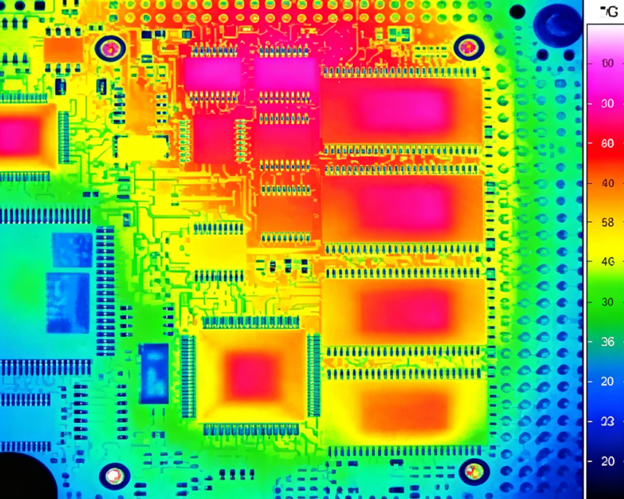
What Common Defects Can PCB Thermal Stress Testing Identify?
Daily finished product appearance inspection cannot find many hidden internal flaws, while standard thermal stress test for PCB can fully expose these potential risks that easily trigger faults in actual use scenes.
- Inner board layer separation: This problem happens due to weak internal pressing connection or residual moisture inside boards, and usually appears in the form of surface bulging and layered separation near board edges and large area copper laying positions.
- Surface copper layer peeling off: Circuit tracks and welding pads separate from the base material, which is mainly caused by unqualified adhesion processing or excessive mismatch of material temperature expansion coefficients.
- Connecting hole internal crack damage: Repeated temperature expansion and contraction will produce tiny cracks inside metal plated through holes and inner connecting holes, further evolving into intermittent circuit connection interruption or thorough circuit breaking faults.
- Welding position fatigue damage: Long term temperature changes will lead to crack generation at the connection positions between electronic parts and PCB surfaces, which greatly shortens the stable service life of assembled finished products.
- Base material body fracture: Rigid circuit boards are more likely to have base material crack damage when enduring super wide range temperature changes, directly destroying the overall structural stability of boards.
- Base material aging and performance decline: Obvious color changes gradual hardening and decreasing insulation performance of board base materials all belong to irreversible aging phenomena caused by long term thermal influence.
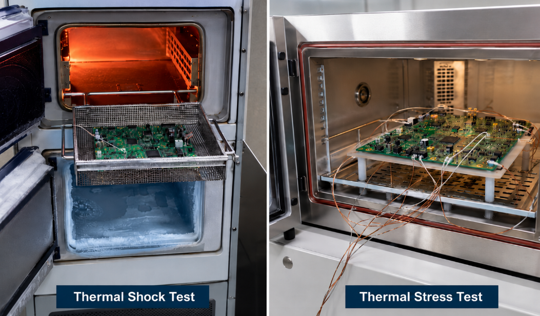
What is the Difference between PCB Thermal Stress Test and Thermal Shock Test?
Many on site technical staff easily mix up thermal stress test for PCB and thermal shock test work, yet these two detection modes differ greatly in temperature adjustment speed internal stress generation ways and actual applicable scenes.
- Speed of temperature switching: Thermal stress test for PCB adopts slow and steady temperature adjustment speed controlled within 1°C to 5°C per minute, giving all internal board materials sufficient time to adapt to ambient temperature changes. Thermal shock test will complete extreme high and low temperature switching within 15 seconds through separate hot and cold storage spaces.
- Core internal stress generation mode: Thermal stress testing mainly accumulates fatigue damage through multiple times of mild expansion and shrinkage actions of materials. Thermal shock testing instantly forms huge instantaneous stress inside boards through rapid temperature difference impact.
- Main detected fault types: Thermal stress testing is good at finding long term accumulated damage such as welding position cracks and inner layer separation after multiple cycles. Thermal shock testing is more suitable for checking brittle structural damage such as connecting hole cracks caused by instant strong impact force.
- Commonly adopted temperature ranges: The conventional temperature range adopted in thermal stress testing stays at -40°C to +125°C, with long standing time at fixed temperature points. Thermal shock testing usually uses wider temperature limits such as-55°C to +150°C, and samples only stay for a short time after reaching preset temperature values.
- Main applicable product fields: Thermal stress testing is widely used to confirm daily stable working performance of civil electronic equipment industrial control devices and common vehicle mounted products. Thermal shock testing is mainly used for performance verification of high precision medical equipment and other products with extremely high safety standards.
What Temperature Parameters Apply to Thermal Stress Test for PCB?
All temperature related data adopted in thermal stress test for PCB will be adjusted according to actual product application fields and followed official testing rules, and all set values are formulated by referring to real daily working ambient conditions.
Low temperature fixed values
- -40°C: Belongs to the most widely adopted standard low temperature parameter, which simulates the lowest ambient temperature that most civil and industrial electronic products may encounter in daily use.
- -55°C: Mostly used for product verification work of high precision equipment that needs to adapt to complex field environments such as outdoor aerial equipment.
- -20°C: Suitable for various indoor fixed use electronic devices that basically do not need to work in low temperature freezing environments.
High temperature fixed values
- +125°C: The mainstream upper limit temperature parameter for industrial control equipment and common vehicle mounted circuit boards, simulating high temperature working states generated by high power operation and closed installation environments.
- +150°C: Reserved for high standard special equipment PCB products that need to keep stable operation under long term ultra high temperature working conditions.
- +85°C: Applied to various daily civil electronic products with low internal heat generation and mild overall working environments.
Fixed temperature standing duration
The standing time after reaching preset highest and lowest temperature points is generally controlled between 15 minutes and 60 minutes. This operation ensures the whole body of tested PCB samples can reach the same ambient temperature, and 30 minutes standing time is recognized as the most balanced setting mode by most industrial rules.
Temperature adjustment speed
The whole heating and cooling process needs to be steadily controlled within 1°C to 5°C per minute. This setting can avoid instantaneous strong temperature impact interference and ensure the testing work focuses on checking long term accumulated thermal stress damage.
Which PCBs Need Thermal Stress Testing and Which Do Not?
It is not necessary to arrange thermal stress test for PCB for all types of circuit board products. The specific arrangement standard depends on product actual use scenes external working environments and overall long term stable operation requirements.
PCB types that must complete thermal stress testing
- High-safety electronic supporting PCBs: PCBs for aerospace, medical precision devices, and automotive safety control systems. Thermal stress testing is mandatory to prevent safety accidents and economic losses from PCB failures.
- PCBs used in harsh external environments: PCBs for outdoor monitoring, field industrial control, and under-vehicle parts. They need thermal stress testing to withstand frequent temperature changes and extreme conditions.
- High-density multi-layer and special structural PCBs: Includes 4-layer+ PCBs, micro-hole, thick copper, and ultra-long integrated PCBs. Their complex structures make thermal stress testing necessary to avoid layer separation and deformation.
- Long-service-life oriented PCBs: PCBs for infrastructure and industrial control designed to work over 5 years. Thermal stress testing ensures long-term reliable operation.
- Power supply and core control PCBs: PCBs for power modules, core control units, and power management. Thermal stress testing is indispensable to avoid equipment malfunctions.
PCB types that can skip thermal stress testing
- Low-cost, short-service-life civil electronic PCBs: Simple-structured PCBs matched with disposable daily electronic gadgets (disposable electronic thermometers, single-use remote controls), low-grade peripheral products (basic USB adapters, simple toy control boards), and low-cost consumer electronics accessories. These products have a short service life (usually less than 1 year) and simple working environments, so thermal stress testing is unnecessary.
- PCBs for indoor stable environment fixed-use equipment: PCBs built into various office equipment (desktop computer motherboards, printer control boards) and household daily electronic devices (TV internal boards, air conditioner remote control main boards) that operate in constant-temperature air-conditioned rooms all year round. The stable ambient temperature eliminates the need for thermal stress testing.
- Single-layer, simple low-density PCBs: PCBs with simple structures, few internal wiring, small copper-clad areas, and no obvious stress concentration points, such as simple LED light control boards, basic switch control PCBs, and low-cost sensor signal transmission boards. Their simple structure makes them less prone to thermal stress damage.
- Early-stage concept verification sample PCBs: Trial-produced PCBs only used to confirm product design feasibility (prototype PCBs for new product development, design verification samples). These samples are not mass-produced and do not need to invest extra time and cost in formal thermal resistance cycle testing.
How Long Does a Standard Thermal Stress Test for PCB Last?
The total time consumed by the whole set of thermal stress test for PCB is mainly decided by the total number of preset temperature cycles fixed standing time and actual temperature switching speed.
In accordance with the unified operating rules of IPC TM 650, when setting 100 complete temperature cycles, 30 minutes fixed temperature standing time and 1°C per minute steady temperature adjustment speed, the continuous running time needed for testing equipment reaches about 100 hours in total.
- Daily civil electronic products: Need to finish 100 to 200 temperature cycles, and the whole testing process takes 100 to 200 hours in total.
- General industrial control supporting products: Need to complete 300 to 500 temperature cycles, corresponding total testing time ranges from 300 hours to 500 hours.
- Vehicle mounted special electronic equipment: The required cycle number is controlled between 500 and 1000 times, and the whole verification work needs 500 to 1000 hours of continuous equipment operation.
- High standard special field equipment: Products with the highest reliability requirements need more than 1000 temperature cycles, so the testing cycle will exceed 1000 hours.
Apart from the continuous running time of core testing equipment, early stage sample sorting work midway repeated performance detection and final finished result sorting work will additionally take up 10 to 20 hours of working time in the whole project flow.
What Equipment is Required for PCB Thermal Stress Testing?
To finish accurate and standard thermal stress tested for PCB work, relevant production and testing teams need to equip matched professional devices to realize precise temperature regulation and real time working state monitoring.
- Programmable temperature cycling testing cabinet: This is the core operating device for the whole testing work. Its adjustable temperature range needs to reach-70°C to +180°C, and it can freely set temperature changing speed and fixed standing time. Built in uniform air flow structures ensure all placed samples receive consistent temperature influence.
- Precision temperature adjusting control unit: Adopts mature closed loop regulation design, with actual temperature control error kept within ±0.5°C. It can automatically run all preset temperature changing sequences without manual repeated parameter adjustment.
- Insulated sample fixing brackets: Special brackets made of non conductive materials are used to fix PCB samples. The structural design will not restrict the normal expansion and shrinkage of boards, and can reserve enough air circulation gaps.
- Real time temperature induction sensors: Small sized high precision thermosensitive parts are pasted on representative testing samples, used to feed back the actual internal temperature of boards, so as to check whether there is deviation between actual temperature and equipment set parameters.
- Electrical function detection instruments: Common multimeter insulation resistance detectors and circuit conduction testing tools are used to record the changes of sample electrical performance before during and after temperature cycling.
- High precision appearance observation tools: Portable magnifying equipment stereo microscopic observation devices and backlight detection auxiliary tools help staff find tiny layering traces and surface tiny crack damage that cannot be seen by naked eyes.
- Whole process data recording system: Matched recording software can automatically store all temperature changing curves completed cycle numbers and actual testing duration data, facilitating later result sorting and product qualification file archiving work.
How to Analyze PCB Thermal Stress Test Results?
Reasonable sorting and judgment of thermal stress test for PCB results need to combine external appearance state observation and internal electrical function detection, and all judgment standards must refer to unified industrial specification requirements.
- External appearance state sorting and judgment: Carefully check all tested samples for surface bulging inner layer separation copper layer peeling off and base material fracture phenomena. All abnormal structural changes that do not conform to IPC unified acceptance rules are directly judged as unqualified products.
- Whole machine electrical function recheck: Re test circuit conduction states internal insulation performance and actual working functions of samples. Phenomena such as unstable circuit connection rising circuit resistance and internal short circuit all prove that thermal stress has caused irreversible damage to boards.
- Microscopic detailed inspection work: Use professional stereo observation equipment to carefully check the internal state of connecting holes welding joint structures and internal material joint positions, so as to find tiny hidden cracks hidden in invisible positions.
- Internal section cutting and observation: For core key testing samples, adopt professional cutting and polishing processing modes to observe the actual bonding state of internal board layers and the complete structure of metal connecting holes from the cross section perspective.
- Compare data with qualified judgment standards: Strictly follow corresponding industrial specifications and customized product technical requirements to finish result confirmation. Products without any structural separation and electrical function failure can be marked as qualified finished products.
- Classify and record all testing data: Clearly mark the final qualified or unqualified state of each group of samples, record specific defect types actual occurrence positions and damage severity in detail, and provide clear optimization direction for follow up board structure design and production process adjustment work.
What Factors Affect the Accuracy of Thermal Stress Test for PCB?
Many external objective conditions will interfere with the final data of thermal stress test for PCB. Controlling these interference factors within reasonable ranges can effectively improve the repeatability and practical reference value of all testing data.
- Internal temperature uniformity of testing cabinet: Unsmooth internal air circulation will lead to obvious temperature differences in different placement positions of samples, making samples bear inconsistent thermal stress intensity and finally generate scattered testing results. Regular internal equipment maintenance and air flow path sorting work are essential.
- Unstable temperature switching speed: Excessively fast temperature adjustment speed will bring additional instantaneous temperature impact, while excessively slow speed cannot reach the expected thermal stress accumulation effect. All actual running speeds must strictly follow preset standard values.
- Non standard sample preprocessing work: Residual oil stains surface scratches and artificial damage generated in the sorting process will cause abnormal defects unrelated to thermal stress changes. All samples need to complete unified cleaning and full appearance inspection before being put into equipment.
- Unreasonable sample fixing mode: Too tight fixing structures will restrict the natural expansion and shrinkage space of PCB boards, and further form extra artificial stress points on boards. Low constraint non conductive fixing modes are the most suitable choice for formal testing work.
- Excessive residual moisture inside base materials: Unfully dried raw materials contain internal moisture, which will quickly form internal expansion impact under high temperature environments and trigger unnatural layering problems. High humidity samples need to finish pre drying treatment in advance.
- Inconsistent raw material batch quality: Differences in internal resin mixing ratio actual copper layer thickness and early pressing compactness of raw materials from different production batches will directly change the natural temperature expansion performance of boards. All comparison testing samples need to adopt raw materials from the same production batch.
- Long term uncalibrated testing equipment: Drift errors will appear in internal temperature sensing parts and core control components after long term continuous use, resulting in actual testing temperature inconsistent with set values. Regular professional precision calibration work needs to be arranged for all testing equipment.
FAQs About Thermal Stress Test for PCB
Q1: How many actual temperature change cycles will ordinary PCB products encounter in daily practical working processes?
A1: Common civil electronic circuit boards will experience 50 to 200 obvious effective temperature change cycles every year. Vehicle mounted and field industrial control matched PCB products may bear 500 to 1000 times of such cycles within one year, which also explains the rationality of cycle quantity setting in formal qualification testing work.
Q2: Is it feasible to carry out thermal stress tested for PCB detection work on circuit boards assembled with complete electronic parts?
A2: Such operation mode is widely adopted in actual industrial testing work. Testing assembled finished boards can effectively verify the long term stable connection performance of welding positions matching adaptation degree of different parts and the overall anti temperature change performance of complete finished products.
Q3: Are thermal stress test operations and conventional temperature cycle detection work the same type of technical verification means?
A3: These two names point to the same set of actual testing work contents. Thermal stress test focuses on explaining the internal material stress change principle generated in the process, while temperature cycle detection is a direct description of the whole external operation flow.
Q4: Are there other replaceable detection ways to finish PCB anti thermal stress performance verification work?
A4: Common alternative ways include internal stress simulation calculation long term constant temperature aging processing and vibration resistance combined detection, yet the actual data obtained from these indirect verification methods cannot replace the real reference value brought by complete thermal stress test for PCB.
Q5: What is the general market charging standard for completing a full set of PCB thermal resistance cyclic testing work?
A5: The overall charging standard is adjusted according to the total number of submitted samples preset cycle times and additional detailed inspection items needed. The market price of conventional standard testing projects ranges from 500 US dollars to 2000 US dollars for each single testing batch, and high standard customized testing projects need to charge extra service fees.
You may also like


Tags: PCB Thermal Stress Test, Thermal Stress Test for PCB, What is a Thermal Stress Test for PCB