

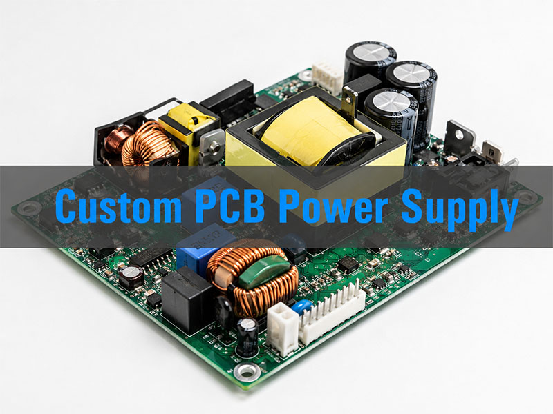
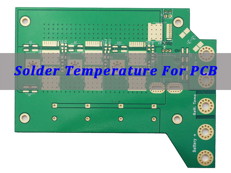
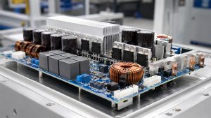
A custom PCB power supply is a printed circuit board designed and manufactured to deliver precise electrical power — specific voltage levels, current capacity, and protection features — tailored to the exact requirements of a product rather than relying on a generic off-the-shelf module. For engineers working on medical devices, industrial controllers, automotive systems, or consumer electronics, getting the power supply right at the PCB level is fundamental to product reliability, thermal performance, and long-term field stability.
This guide covers everything engineers need to know about custom PCB power supply design and wholesale assembly: material selection, layer stack-up, copper thickness, surface finish options, DFM best practices, and how to choose a manufacturing partner who can support you from first prototype through high-volume production.
At EBest Circuit (Best Technology), we have spent 20 years working directly with engineers on exactly this type of project. Every order is handled by a dedicated team of one business partner and three specialized engineers — covering R&D, PCB process, and PCBA assembly — so your technical questions get engineering answers, not sales responses. We hold ISO 9001, ISO 13485, IATF 16949, and AS9100D certifications, run our own PCB and PCBA factory, and consistently deliver full PCBA within 1.5 weeks. If you have a project in mind, feel free to reach out to our team at sales@bestpcbs.com — we are happy to review your requirements and provide a practical assessment.
Why Engineers Choose Custom PCB Power Supply Boards?
Off-the-shelf power supply modules are a convenient starting point, but they rarely satisfy the exacting demands of modern electronics. Whether you are developing a medical device, an industrial controller, automotive electronics, or next-generation consumer hardware, a custom PCB power supply allows you to optimize every parameter — voltage rails, switching frequency, thermal dissipation, EMI shielding, footprint, and reliability — to match your exact application.
Engineers worldwide increasingly choose custom designs for these concrete reasons:
- Precise Power Rails: Define multiple voltage outputs, tight tolerances, and load-step response exactly as your BOM demands — no compromises from a generic module.
- Thermal Optimization: Position power components, copper pours, and thermal vias exactly where thermal simulation says they need to be. Metal-core (aluminum/copper) substrates are available for high-power density designs.
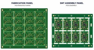
- Form-Factor Freedom: From 3×3 mm microboards to 580×890 mm production panels, custom PCBs fit your mechanical envelope — not the other way around.
- IP Protection: Your custom design stays proprietary. No competitor can buy the same module and replicate your product performance.
- Cost-Efficient Scaling: A custom BOM-optimized design reduces unit cost significantly at volume. Wholesale PCBA is where the real savings are realized.
- Compliance-Ready Design: Design for UL, CE, IEC 62368, or IATF16949 from day one, with an experienced engineering partner who understands certification requirements.
Power Supply PCB Design Essentials
A high-performance custom power supply PCB is the result of dozens of carefully balanced decisions. Below are the most critical areas where design choices directly affect reliability, efficiency, and manufacturability.
1. Topology Selection
The power conversion topology shapes every subsequent design decision. For isolated designs — such as medical or industrial applications — flyback, LLC resonant, or phase-shifted full-bridge are popular choices. For non-isolated point-of-load (POL) regulators, synchronous buck or multi-phase buck are industry standards. Your selection affects transformer design, control IC selection, switching node layout, and EMC strategy.
2. Layer Stack-Up and Current Carrying Capacity
Power supply PCBs carrying more than 5 A require careful stack-up planning. Wide power planes, thick copper, and strategic via stitching keep IR drop and thermal rise within spec. For high-current designs, our manufacturing supports outer copper up to 10 oz (standard) and up to 28 oz (advanced prototype) — one of the highest capabilities available from a China-based manufacturer.
3. EMI Control Layout
Switching power supplies are inherently noisy. The PCB layout must minimize high-di/dt loop areas, place input capacitors as close as possible to the switch nodes, separate analog and power ground planes, and route gate-drive traces with care. A key rule of thumb: the highest-frequency current loop (e.g., MOSFET drain–capacitor–MOSFET source) must be minimized in physical area. For every doubling of loop area, radiated EMI increases approximately 6 dB — enough to fail FCC/CE limits.
4. Impedance Control and Signal Integrity
If your power supply includes digital control (digital PWM, PMBus, I²C), controlled impedance traces are critical. Our standard capability holds impedance to ±5 Ω for values below 50 Ω, and ±10% for 50 Ω and above. Advanced prototype tolerance reaches ±4 Ω / ±6%.
5. Thermal Via Strategy
Thermal vias under power pads (QFN, DFN, TO-263) are essential for junction-temperature management. Proper via fill, pitch, and diameter selection prevents solder voiding while maximizing thermal conductance. Our engineering team provides via-fill recommendations as part of every DFM report.
Material and Layer Selection for Power Supply PCBs
Material selection is the single most impactful decision for long-term power supply reliability. Different applications demand different substrates.
| Material Type | Tg / Key Property | Best Application | Available Brands |
|---|---|---|---|
| FR4 Standard Tg | 130–140 °C | Consumer, low-temp industrial | KB 6160, Shengyi S1141 |
| FR4 Mid Tg | 150 °C | Industrial, higher ambient | KB 6165, Isola IT158, S1000H |
| FR4 High Tg | 170–180 °C | Automotive, high-load power supply | IT180A, S1000-2M, FR408, TU-768 |
| High CTI | CTI ≥ 600 V | High-voltage isolated PSU | S1600L, KB-6165C |
| High-Speed / Low-Loss | Low Dk/Df | GaN/SiC PSU, switching >1 MHz | M4/M6/M7, TU-872SLK, IT-958 |
| Metal Core (Aluminum) | 0.3–6 W/m·K thermal conductivity | LED drivers, high-power PSU | 1100/5052/6061 alloy, Bergquist |
| Metal Core (Copper) | Up to 12 W/m·K (advanced) | Ultra-high-power density designs | Pure copper substrate |
Most power supply designs fall in the 4–8 layer range. Complex digital-power hybrid designs for servers or telecom can reach 16–24 layers with embedded planes for PDN (Power Distribution Network) optimization. Our standard capability covers 1 to 50 layers, with up to 100 layers available on engineering review.
EBest Circuit Manufacturing Capabilities
When you order a customized power supply PCB assembly from EBest Circuit, you benefit from one of the most comprehensive process capability tables available. The data below is drawn directly from our certified process capability documentation.
| Parameter | Standard Capability | Advanced (Prototype) |
|---|---|---|
| Layer Count | 1–50 layers | Up to 100 layers (on review) |
| Board Thickness | 0.4 mm – 6 mm | 0.15 mm – 10 mm |
| Outer Copper Thickness | 0.5 oz – 10 oz | 0.5 oz – 28 oz |
| Inner Copper Thickness | 0.5 oz – 6 oz | 0.5 oz – 20 oz (≥12 oz on review) |
| Laser Drill Min. Diameter | 0.10 mm | 0.070 mm |
| Mechanical Drill Range | 0.15 mm – 6.5 mm | 0.15 mm minimum |
| Min. Board Size | 10 × 10 mm | 3 × 3 mm |
| Max. Board Size (≥3 layers) | 580 × 762 mm | 580 × 1220 mm |
| Min. Line Width / Spacing | 3/3 mil (outer) | 2/2 mil (outer) |
| Impedance Tolerance | ±5 Ω / ±10% | ±4 Ω / ±6% |
| Warp and Twist (Bow) | ≤ 0.75% | ≤ 0.50% |
| Max. Test Voltage | 5,000 V DC / 3,000 V AC | — |
| Metal Core (Al/Cu) | 1–6 layers, 0.5–5 mm thick | >6 layers (on review) |
| Back-Drill Depth Precision | ±0.1 mm | — |
| Thermal Conductivity (Metal Core) | 0.3–6 W/m·K | Up to 12 W/m·K |
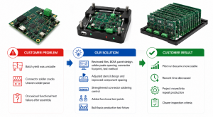
DFM Analysis: How We Help Engineers Avoid Costly Mistakes
Design for Manufacturability (DFM) review is not a checkbox — it is the single most valuable service we provide before a single PCB is fabricated. Our team carries 20 years of PCB/PCBA engineering experience and performs a thorough pre-production audit that covers:
- Gerber vs. BOM cross-check: Verify that every component in your BOM has a corresponding land pattern in the Gerber, with correct polarity markings.
- Copper clearance and creepage compliance: For high-voltage power supplies, IPC-2221 and IEC 60950/62368 clearance and creepage distances are checked against your isolation requirements.
- Drill-to-copper and annular ring analysis: Flag any drills that violate minimum annular ring or drill-to-copper spacing for your selected laminate.
- Solder mask opening audit: Prevent solder bridging and insufficient-solder defects by verifying SM opening ratios against IPC-7527 stencil recommendations.
- Via-in-pad and thermal relief review: Confirm that thermal vias are properly specified (filled vs. unfilled) and that power pad connections use appropriate thermal relief or solid tie.
- Component courtyard conflict detection: Identify component-to-component spacing violations that would prevent standard pick-and-place nozzle access.
- BOM optimization recommendations: Flag obsolete, single-source, or long-lead-time components and suggest qualified alternates from our 1,000+ supply chain partners.
- Impedance stack-up verification: For controlled-impedance designs, model your stack-up against the target Dk of the selected material and confirm trace widths.
Every project receives a formal written DFM Pre-Screening Report before production is approved. Issues are ranked by severity — Critical, Major, or Advisory — so your team can make informed decisions quickly. This service is included in our engineering support at no additional charge.
Surface Finish Options for Power Supply PCBs
Surface finish choice directly affects solderability, shelf life, contact resistance, and overall long-term reliability. Here is a comparison of the most relevant finishes for power supply applications:
| Surface Finish | Thickness | Key Advantage | Best Application |
|---|---|---|---|
| Lead-Free HASL | 2–40 µm | Low cost, excellent solderability | Standard industrial PSU, cost-sensitive runs |
| ENIG (Immersion Gold) | Ni: 3–8 µm / Au: 0.025–0.125 µm | Flat surface, IC-compatible, long shelf life | High-density SMT, BGA, fine-pitch power modules |
| Immersion Tin | 0.8–1.5 µm | RoHS, press-fit connector compatible | Automotive PSU with press-fit connectors |
| Immersion Silver | 0.2–0.4 µm | Excellent flatness, wire-bondable | High-frequency/RF supply hybrids |
| OSP | 0.1–0.3 µm | Ultra-flat, lowest cost, RoHS | Reflow-only assemblies with short storage window |
| ENEPIG | Ni: 3–8 µm / Pd: 0.05–0.125 µm / Au: 0.025–0.125 µm | Wire-bond + solder compatible, no black pad risk | Hybrid power modules with wire bonding |
| Hard Gold (Edge Finger) | 0.1–1.27 µm | Wear-resistant, low contact resistance | Card-edge connectors, test points |
One-Stop PCBA Assembly: From Bare Board to Tested Unit
Our core value proposition is the full integration of PCB fabrication, component procurement, SMT/through-hole assembly, and functional testing under one roof. This eliminates the coordination overhead, quality grey-zones, and lead-time waste that come from splitting your supply chain across multiple vendors.
Step 1 — Engineering Review and DFM Report Your Gerber, BOM, and assembly drawings are reviewed by our engineering team. A written DFM report is issued within 24–48 hours for standard complexity designs.
Step 2 — Component Procurement We source 100% of your BOM through our 1,000+ verified supply chain partners. All components are checked for authenticity and traceability. Counterfeit screening is included for ICs and passives on aerospace and medical builds.
Step 3 — PCB Fabrication Our own factory produces the bare boards to your exact specification. No broker — direct factory control from inner-layer imaging through final electrical test.
Step 4 — SMT and Through-Hole Assembly Automated SMT with AOI (Automated Optical Inspection) after paste printing and after reflow. Manual through-hole and selective soldering for connectors and large power components.
Step 5 — Inspection: X-Ray, AOI, and Visual BGA and QFN solder joints are verified by X-ray inspection. 3D AOI is applied on all boards. IPC-A-610 workmanship standard is applied by default.
Step 6 — Functional and Electrical Testing In-Circuit Testing (ICT), flying probe, and functional test per your test specification. Power supply output voltage, ripple, load regulation, and efficiency can all be measured and logged.
Step 7 — Digital Traceability and Shipping Our digital manufacturing system provides material and batch traceability within 5 seconds. Full shipping documentation, Certificate of Conformance, and test records accompany every order.
Wholesale and Prototype: Flexible Volume for Every Stage
One of the most common pain points for engineers is finding a PCBA partner who can serve them cost-effectively across all stages of a product’s lifecycle — from the first 5-piece engineering sample to a 10,000-piece production run. EBest Circuit is purpose-built to support this entire journey.
- Prototype (1–10 pcs): Minimum 1 piece. Rapid prototyping with DFM engineering support. Designed for design validation and debugging loops.
- Small Batch (10–500 pcs): Pre-production validation builds. Fixed setup costs spread across units. Suitable for crowdfunding fulfillment or pilot programs.
- Volume / Wholesale (500+ pcs): Competitive unit pricing with full SMT line utilization. Long-term blanket order contracts available for supply chain security.
Our standard full-service PCBA lead time is 1.5 weeks (approximately 10–12 business days) from the date your Gerber files, BOM, and purchase order are confirmed. This covers PCB fabrication, component procurement (assuming stock availability), SMT assembly, AOI, and final testing. Express options are available for urgent projects.
Certifications and Quality System
Quality is a documented, audited, and continuously improved system. EBest Circuit holds the following certifications, each maintained through regular third-party audits:
- ISO 9001:2015 — General quality management system
- ISO 13485:2016 — Medical device supply chain quality
- IATF 16949:2016 — Tier 1 automotive supplier process control and PPAP documentation
- AS9100D — Aerospace and defense supply chain requirements
- IPC-A-610 — PCB assembly workmanship standard
- RoHS / REACH — Environmental compliance
The IATF 16949 certification means our processes meet the highest standards for process control in the automotive industry. The AS9100D certification covers aerospace and defense supply chain requirements. ISO 13485 ensures our quality system is compliant for medical device supply chains — all relevant certifications for engineers who need their power supply boards to meet the most demanding end-market requirements.
Our digital workshop management system enables real-time tracking of material lots, production batches, and individual board serial numbers. In the event of a field return or audit, full manufacturing history can be retrieved in under 5 seconds — an essential capability for automotive and medical customers.
Why 1,800+ Engineers Choose EBest Circuit?
20 years of specialized PCBA history. EBest Circuit (Best Technology) has been focused on PCB fabrication and PCBA assembly for over two decades. We have supported more than 10,000 engineers and 1,800+ customers worldwide across medical, automotive, industrial, aerospace, and consumer electronics sectors.
The 1 Business Partner + 3-Engineer Technical Team model. Every new project is assigned a dedicated team: one experienced business partner who manages communication and timelines, plus a three-engineer technical team comprising a 20-year R&D engineer, a PCB process specialist, and a PCBA assembly engineer. This means:
- Engineering questions are answered by engineers, not by a sales representative reading from a spec sheet.
- DFM findings are reviewed by a multi-discipline team, not a single generalist.
- Your project manager has technical authority to approve or flag issues without internal escalation delays.
- Communication is consolidated — one contact, no information loss between departments.
Own factory with direct quality control. We own both our PCB fabrication facility and our PCBA assembly line. This vertical integration gives us direct control over every substrate that goes into your board — nothing is delegated to a sub-contractor we cannot audit. At the same time, our 1,000+ component supply chain partners ensure broad BOM coverage and transparent pricing for wholesale orders.
If you are ready to move your power supply design from schematic to production, our engineering team is ready to review your files and provide a technical assessment and competitive pricing — typically within 24 hours. Just feel free to send your Gerber files, BOM, and project requirements to sales@bestpcbs.com.
Our team of dedicated engineers — not automated forms — will personally review your specifications and respond with a tailored recommendation. Whether you need a 5-piece prototype to validate your design or a 10,000-piece wholesale production run to meet a launch deadline, EBest Circuit has the process capability, certifications, and engineering depth to deliver on time.
FAQs About Custom PCB Power Supply
What is the minimum order quantity for a custom PCB power supply?
EBest Circuit supports prototype orders from as little as 1 piece. There is no minimum order quantity restriction for engineering samples. Wholesale pricing tiers begin at approximately 500 pieces, with the most competitive rates available from 5,000 pieces and above.
How long does PCBA assembly take for a custom power supply?
Our standard full-service PCBA lead time is 1.5 weeks (approximately 10–12 business days) from the date your Gerber files, BOM, and purchase order are confirmed. This includes PCB fabrication, component procurement, SMT assembly, AOI, and final testing. Rush options are available for time-critical projects.
Do you provide DFM review?
Yes — DFM review is included as a standard part of our engineering service. Every project receives a formal written DFM Pre-Screening Report before production is approved, covering Gerber verification, clearance/creepage compliance, via-in-pad review, component spacing, and BOM optimization recommendations.
Can you manufacture metal-core PCBs for high-power applications?
Yes. Our capability covers aluminum-core PCBs (alloys 1100, 1050, 2124, 5052, 6061) and copper-core PCBs for ultra-high thermal conductivity applications. Standard thermal conductivity ranges from 0.3 to 6 W/m·K, with advanced capability up to 12 W/m·K. Metal core boards support 1–6 layers in standard process (more on review).
Which certifications does EBest Circuit hold?
EBest Circuit is certified to ISO 9001:2015, ISO 13485:2016, IATF 16949:2016, and AS9100D. These certifications are maintained through regular third-party audits.
How do you ensure component authenticity for wholesale orders?
All components are sourced through 1,000+ verified supply chain partners. For aerospace and medical builds, active counterfeit screening is performed including X-ray inspection and full lot traceability. Certificates of Conformance are provided with every shipment.
You may also like
Tags: Custom PCB Power Supply, customized power supply PCB assembly wholesale