

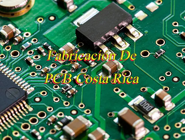
Are you tired of unreliable lead times, inconsistent quality, and hidden risks during fabricación de PCB that derail your prototypes and production schedules? In this guide, we break down the real challenges in diseño y fabricación de PCB, explain el proceso de fabricación de PCB in clear steps, compare top local suppliers, and show how EBest delivers stable, certified, and fast fabricación de PCB a medida with free DFM analysis and flexible support. By the end, you will know exactly how to choose a trusted PCB partner and why EBest is the top choice for reliable fabricación de PCB in Costa Rica and globally.
Why Choose EBest for Your Fabricación de PCB Needs?
When you need professional and stable fabricación de PCB, EBest Circuit is your best choice. Here are why choose us for your fabricación de PCB needs:
- Ultra‑fast lead time: Urgent prototype orders ship within 24 hours to keep your project on track.
- Consistent high quality: Full process inspection and zero‑defect control for reliable end products.
- Complete industry certifications: IATF 16949, ISO 9001, ISO 13485, AS9100D, REACH, RoHS, UL for global market access.
- Free DFM analysis for every project: Fix design risks early and avoid costly reworks.
- Flexible MOQ for prototypes: Support small‑batch trials with no unnecessary barriers.
- Full customization: Expert fabricación de PCB a medida for any layer, material, or performance requirement.
- One‑stop service: Covering diseño y fabricación de PCB, assembly, components, and testing.
- Stable mass production capacity: Consistent quality between samples and volume orders.
- Strong engineering support: In‑house technical team to solve complex design and production issues.
- High‑precision capabilities: HDI, high‑TG, heavy copper, high‑frequency, and rigid‑flex PCBs supported.
- Full traceability: Material and production records for medical, automotive, and aerospace projects.
- Global logistics support: Reliable delivery to Costa Rica and worldwide destinations.
We put your project success first with professional fabricación de PCB solutions you can trust.
Our Comprehensive Diseño y Fabricación de PCB Services
EBest provides full‑cycle diseño y fabricación de PCB for global customers.
- PCB Design: Layout, impedance control, and schematic support.
- PCB Prototype: Rapid small‑batch production.
- Mass Production: Stable high‑volume manufacturing.
- Component Sourcing: Authentic components with full traceability.
- PCB Assembly: SMT, through‑hole, and functional testing.
All services include customization and free DFM reports for design optimization.
Quality Certifications for Reliable Fabricación de PCB
Our certifications guarantee compliant and trustworthy fabricación de PCB.
- IATF 16949: Automotive electronics standard.
- ISO 9001:2015: Quality management system.
- ISO 13485:2016: Medical device quality system.
- AS9100D: Aerospace and high‑reliability standard.
- REACH & RoHS: Environmental compliance.
- UL: International safety certification.
These certifications meet global industry and market requirements.
Our Production Capabilities for Fabricación de PCB a Medida
| Capability | Specification |
| Monthly Capacity | 260,000 ft² / 28,900 m² |
| Board Types | FR4, metal core, ceramic, flex, rigid‑flex, RF, high‑frequency |
| Layer Count | 1–78 layers, HDI supported |
| Special Features | Heavy copper, high TG, ultra‑thin, impedance control, IC substrates |
| Quick Turn | 24‑hour expedite service for urgent orders |
Common Challenges in El Proceso de Fabricación de PCB & How We Solve Them
Engineering, design, and procurement teams frequently face costly, time‑consuming obstacles during el proceso de fabricación de PCB. We deliver clear, actionable solutions to keep your project on track.
- Designs that fail manufacturing validation: Our dedicated engineering team provides free DFM analysis to identify and correct layout, spacing, impedance, and material conflicts before production, eliminating reworks and delays.
- Excessively long lead times for prototype development: We offer dedicated rapid prototype lines and 24‑hour expedite services to support urgent testing, product launches, and time‑sensitive development cycles.
- Inconsistent quality between prototypes and mass production: We use identical materials, production lines, and quality standards for both samples and mass production, ensuring stable performance and full compatibility at any volume.
- Lack of certifications for medical, automotive, and aerospace use: Our facilities hold IATF 16949, ISO 13485, AS9100D, UL, RoHS, and REACH certifications, supporting regulated industries with full compliance and audit-ready documentation.
- Inflexible order requirements for small-batch R&D projects: We support flexible MOQ for prototypes and pre-production runs, letting you validate designs and test markets without high upfront commitments or waste.
- Unclear communication and slow technical support: Our in-house engineering team provides direct, timely technical support throughout design, production, and delivery, keeping you informed and resolving issues quickly.
When you need consistent, professional fabricación de PCB, EBest delivers proven, end-to-end solutions tailored to your needs.
Top 10 Fabricación de PCB Manufacturers in Costa Rica
| Company Name | Main Products & Services | Production Process | Lead Time |
| EBest Circuit | Full diseño y fabricación de PCB, HDI, high-frequency, rigid-flex, fabricación de PCB a medida, assembly | 1–78 layers, HDI, heavy copper, high TG, RF, MCPCB, ceramic | Prototype: 2–5 days; Urgent: 24 hours; Mass: 7–10 days |
| Electrónica PCB Costa Rica | Standard FR4 PCB, prototypes, small-batch production | 1–4 layer standard FR4 | Prototype: 5–7 days; Mass: 10–15 days |
| PCB Solutions CR | Single/double-sided PCB, low-volume assembly | 1–2 layer basic rigid PCB | Prototype: 6–8 days; Mass: 12–18 days |
| TechCircuit CR | Rigid PCBs for consumer electronics | 1–4 layer standard PCB | Prototype: 5–7 days; Mass: 10–15 days |
| Centroamérica PCB | Simple rigid boards, local assembly | 1–2 layer basic PCB | Prototype: 7–10 days; Mass: 15–20 days |
| PCB Prototipos CR | Fast prototypes, basic 1–2 layer boards | 1–2 layer simple PCB | Prototype: 3–5 days; Mass: Not supported |
| Electronic Manufacturing CR | Through-hole assembly, basic rigid PCBs | 1–4 layer standard PCB | Prototype: 6–9 days; Mass: 12–18 days |
| PCB Industrial CR | Industrial control boards, standard rigid PCB | 1–4 layer industrial PCB | Prototype: 5–8 days; Mass: 10–16 days |
| PCB Médico CR | Basic medical PCBs, simple rigid boards | 1–4 layer medical grade PCB | Prototype: 7–10 days; Mass: 14–20 days |
| PCB Auto CR | Basic automotive boards, standard rigid PCB | 1–4 layer automotive PCB | Prototype: 6–9 days; Mass: 12–18 days |
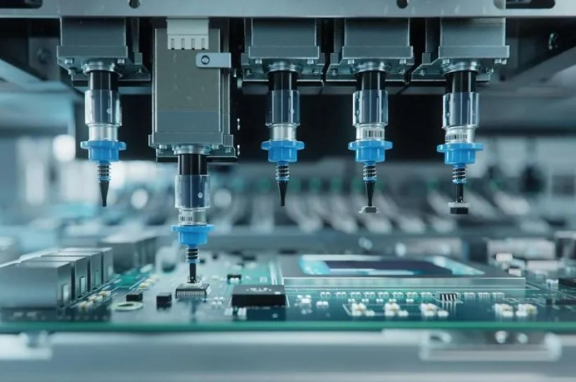
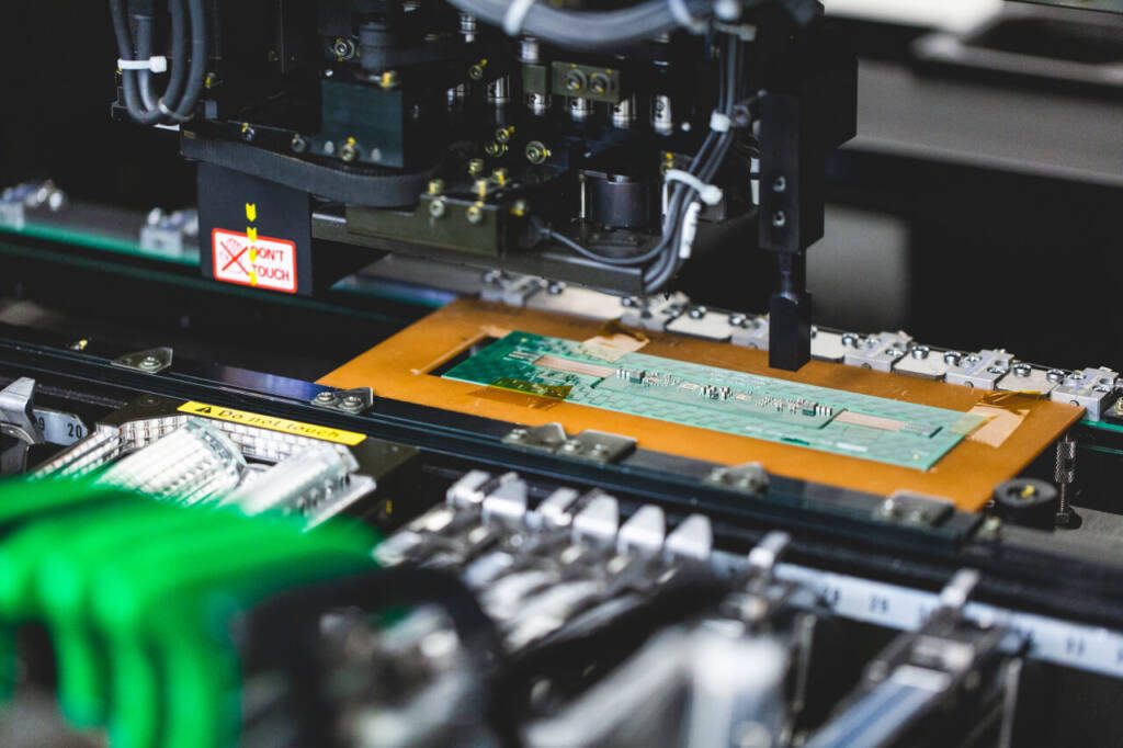
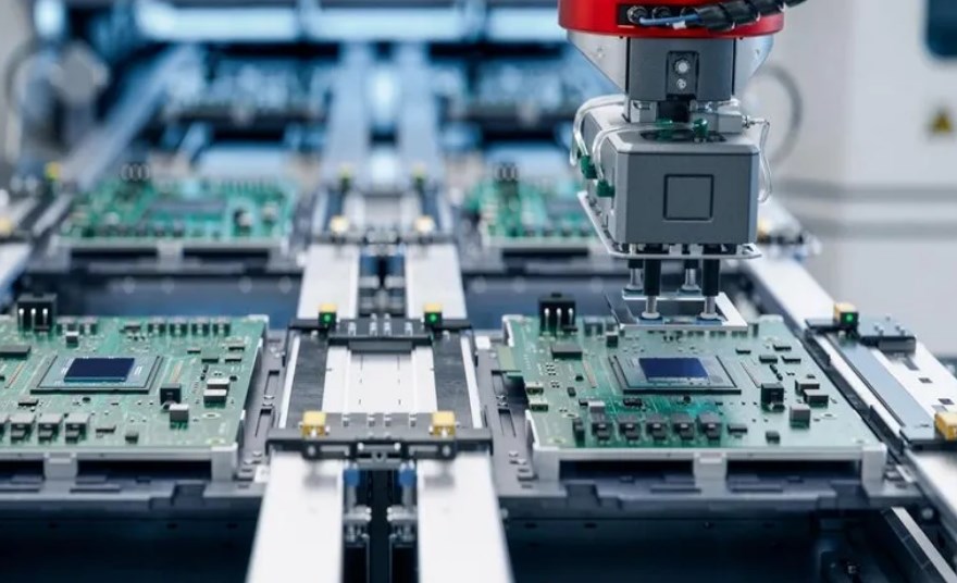
How Does El Proceso de Fabricación de PCB Work Step by Step?
El proceso de fabricación de PCB follows a strict, repeatable engineering workflow to ensure reliability and consistency for every custom board. Below is the complete, easy-to-understand production flow.
- Receive design files: Gerber data, BOM, drill files, and stack-up details.
- Perform free DFM analysis to check for design errors, spacing, impedance, and manufacturability.
- Confirm materials and specifications: Copper thickness, substrate type, surface finish, and layer count.
- Laminate core and prepreg materials under high temperature and pressure.
- Image circuit patterns onto the inner layers using dry film and exposure.
- Etch to remove excess copper and form the circuit pattern.
- Optical inspection (AOI) to detect defects in inner layers.
- Layer stacking and lamination for multilayer PCBs.
- CNC drilling for vias and through-holes.
- Electroless copper plating and electroplating to build conductive paths.
- Outer layer imaging, etching, and tin plating.
- Solder mask application for insulation and protection.
- Surface finish treatment: ENIG, HASL, immersion silver, or other required finishes.
- Silkscreen printing for labels, logos, and component indicators.
- Electrical testing (ET) to check open/short circuits.
- Final visual inspection and quality verification.
- Packaging, labeling, and shipment according to customer requirements.
Industry Applications for High‑Performance PCB Solutions
We deliver targeted fabricación de PCB and fabricación de PCB a medida for four high‑demand industries, with fully customized designs, certified quality, and optimized performance for real‑world use.
Automotive Electronics
We provide fabricación de PCB a medida including heavy copper PCBs and metal core PCBs (MCPCB) for electric vehicle controllers, battery management systems (BMS), and automotive sensors.
All boards are built under IATF 16949 standards, with stable performance in high‑temperature and vibration environments. Custom layer counts, materials, and thermal designs are fully supported to meet strict automotive requirements.
Medical Devices
Our fabricación de PCB a medida delivers rigid‑flex PCBs, ultra‑thin PCBs, and high‑precision boards for patient monitors, diagnostic equipment, and portable medical devices.
Certified to ISO 13485, these boards offer reliable signal transmission, long‑term stability, and full traceability.Custom specifications ensure compatibility with strict medical regulatory and safety demands.
Industrial Control & Automation
We offer fabricación de PCB a medida with high TG, multilayer, and heavy copper structures for PLCs, industrial drives, robotics, and automation control systems.
These PCBs resist high temperatures, electrical interference, and long‑term continuous operation.Custom designs improve stability and extend service life in harsh industrial environments.
Communications & Servers
Our fabricación de PCB a medida provides high‑speed, impedance‑controlled, and high‑frequency PCBs for 5G equipment, data center servers, routers, and communication base stations.
These boards ensure stable signal transmission, low loss, and reliable performance for high‑speed data processing. Full customization supports complex stack‑up, impedance control, and high‑density layout requirements.
All industry solutions include free DFM analysis and full engineering support to bring your custom PCB designs.
How to Select the Best Partner for Diseño y Fabricación de PCB?
Choosing a reliable provider for diseño y fabricación de PCB directly affects product quality, lead time, and project success. Use these key criteria to evaluate and select your ideal partner.
- Verify industry‑relevant certifications: Check for IATF 16949 (automotive), ISO 13485 (medical), AS9100D (aerospace), ISO 9001, RoHS, REACH, and UL to ensure compliance and quality stability.
- Confirm comprehensive technical and manufacturing capabilities: Ensure the supplier supports HDI, high‑TG, heavy copper, rigid‑flex, high‑frequency, and fabricación de PCB a medida to match your design requirements.
- Check for professional DFM and engineering support: A qualified partner must provide free DFM analysis to optimize designs, reduce risks, and prevent costly reworks during production.
- Evaluate lead time and quick‑turn services: Reliable suppliers offer fast prototype turnaround and 24‑hour expedite services to support urgent development and product launches.
- Review quality control and testing systems: Confirm full process inspection, AOI, electrical testing, and traceability systems to ensure consistent quality between prototypes and mass production.
- Check one‑stop service coverage: Prefer suppliers offering full diseño y fabricación de PCB, component sourcing, assembly, and testing to simplify management and reduce coordination risks.
- Evaluate MOQ flexibility for prototypes and small batches: A customer‑focused manufacturer supports flexible MOQ for R&D and pre‑production trials without unnecessary restrictions.
- Review real customer cases and industry experience: Choose partners with successful applications in your target industry (automotive, medical, industrial, communications) for better technical matching.
- Check communication and technical support efficiency: Direct engineering support and responsive service help resolve issues quickly and keep projects on schedule.
- Confirm stable supply chain and material traceability: Ensure authentic raw materials, full batch traceability, and stable supply to avoid production delays or quality risks.
- Evaluate global logistics and after‑sales support: Reliable delivery, packaging, and after‑sales service ensure smooth receipt and support for your fabricación de PCB projects.
FAQ: Preguntas Frecuentes sobre Fabricación de PCB en Costa Rica
Q1: What is the typical lead time for fabricación de PCB?
A1: Standard prototypes: 3–5 days; urgent orders: 24 hours.
Q2: Do you offer fabricación de PCB a medida?
A2: Yes, we fully support custom layers, materials, thickness, impedance, and special performance requirements.
Q3: Is free DFM analysis included?
A3: Yes, free DFM is provided for all orders to optimize design and avoid production risks.
Q4: Can you produce HDI and high‑frequency PCBs?
A4: Yes, HDI, high‑TG, heavy copper, RF, and high‑frequency boards are all available.
Q5: Do you provide PCB assembly services?
A5: Yes, we offer one‑stop diseño y fabricación de PCB + assembly + testing.
Contact EBest for Your Fabricación de PCB Project
EBest provides professional fabricación de PCB, diseño y fabricación de PCB, and fabricación de PCB a medida with certified quality and fast delivery.We support customization and include free DFM reports for every project. Contact us now: sales@bestpcbs.com to get a free quote for your project!
You may also like

Tags: diseño y fabricacion de pcb, el proceso de fabricacion de pcb, fabricacion de pcb, fabricacion de pcb a medida, fabricacion de pcb costa rica