

What are DBC/DCB ceramic substrates?
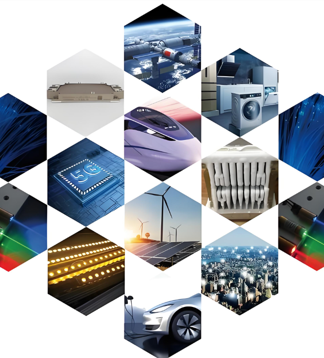
DBC/DCB ceramic substrates are copper-on-ceramic platforms used inside power semiconductor packages to carry high current, isolate high voltage, and move heat into a heatsink with low thermal resistance. If you work with IGBT modules, SiC MOSFET modules, inverters, or high-power converters, they are one of the most common “workhorse” substrate choices because they combine electrical insulation and thermal conduction in one compact layer stack.
A ceramic substrate provides dielectric isolation, while thick copper layers on one or both sides provide low-resistance current paths and a mounting surface for chips, sinter, or solder. That combination is hard to achieve with standard PCB materials at the same voltage and power density.
What problem do they solve in IGBT and SiC module packaging?
Power devices generate heat and also demand safe isolation. A power package must do four jobs at once: conduct current, withstand kilovolts, spread heat, and survive thermal cycling. A copper-on-ceramic substrate is purpose-built for this “four-in-one” requirement.
What does “DBC” vs “DCB” mean in real projects?
In most purchasing and engineering discussions, “DBC” and “DCB” are used interchangeably. You will see both terms on drawings, RFQs, and datasheets. Practically, what matters is the material stack (Al2O3/AlN/Si3N4), copper thickness, ceramic thickness, and the reliability target (thermal cycling, partial discharge margin, and mechanical robustness).
Why do power modules prefer DBC/DCB ceramic substrates over standard PCBs?
They win because they deliver high current + high voltage isolation + strong heat flow in a footprint that stays stable across temperature swings.
How do they handle high current, high voltage isolation, and heat together?
- High current: Copper layers are much thicker than typical PCB copper, so I²R losses drop and temperature rise is easier to control.
- High voltage: Ceramic provides strong dielectric isolation, supporting the separation between high-side and low-side copper patterns.
- Heat removal: The ceramic layer conducts heat down to a baseplate or heatsink while copper spreads heat laterally.
What makes ceramic + copper “package-grade” compared to PCB-grade?
A standard FR-4 PCB can route signals nicely, but power packages are about controlled thermal paths and insulation integrity over years of cycling. Ceramic substrates are designed for harsh operating profiles, including repeated temperature swings and high junction temperatures.
How does the DBC/DCB process work (in simple steps)?
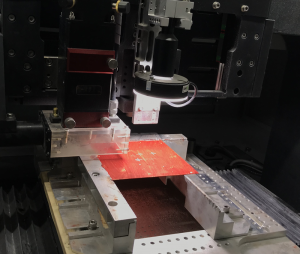
DBC/DCB uses a bonding method that creates a strong interface between copper foil and ceramic. Then the copper is patterned (etched) into circuits, and the finished substrate is plated or surface-finished as needed for die attach and wire bond.
Step-by-step (beginner-friendly)
- Ceramic selection: Choose Al2O3, AlN, or Si3N4 based on cost, thermal needs, and mechanical strength targets.
- Copper bonding: Copper foil is bonded to the ceramic at high temperature under controlled atmosphere to form a reliable copper–ceramic interface.
- Circuit patterning: The copper is etched into traces, pads, and isolation gaps.
- Surface finish: Common finishes include Ni/Au or other plating stacks depending on die attach, soldering, and bondability requirements.
- Inspection: Flatness, copper thickness, etch quality, and dielectric integrity are checked to match the application risk level.
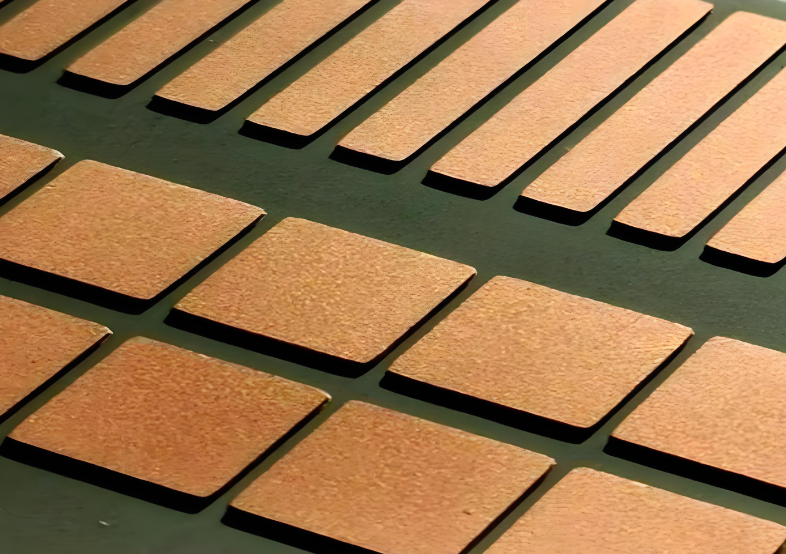
Single-sided vs double-sided copper
Single-sided is used for simpler thermal and circuit needs. Double-sided copper is common in modules because it can improve heat spreading, stiffness, and interconnect options. The “right” choice depends on your mechanical stack and how you mount the substrate to the baseplate or heatsink.
Which ceramic is better for DBC/DCB: Al2O3 vs AlN vs Si3N4?
If you need value and proven supply chains, start with alumina. If you are heat-limited, AlN usually moves the needle. If your priority is mechanical toughness and thermal shock resistance, Si3N4 often leads.
| Material | Best for | Typical strengths | Trade-offs |
|---|---|---|---|
| Alumina (Al2O3) | Mainstream power modules | Cost-effective, mature, widely available | Lower thermal conductivity vs AlN; more brittle than Si3N4 |
| Aluminum Nitride (AlN) | Thermal-limited designs | High thermal conductivity for lower thermal resistance | Higher cost; handling and processing needs more control |
| Silicon Nitride (Si3N4) | High reliability, cycling-heavy environments | High mechanical strength; strong thermal shock resistance | Premium material; availability may vary by spec |
When is alumina the smartest choice?
Choose alumina when your thermal budget is reasonable and you want a robust, cost-controlled BOM. Many industrial inverters, motor drives, and general power conversion stacks land here because it balances performance and procurement stability.
When do AlN and Si3N4 justify the premium?
AlN DBC substrates are a common upgrade path when junction temperature margin is tight, or when you want lower thermal resistance without enlarging the package. Si3N4 DBC substrates often show up when reliability under cycling is the dominant KPI—such as traction inverters, automotive environments, and harsh duty profiles.
What copper thickness and ceramic thickness should you specify for DBC/DCB?
Pick copper thickness based on current density and heat spreading goals. Pick ceramic thickness based on voltage isolation margin and mechanical stack constraints. Avoid “one-size-fits-all” defaults, because the wrong thickness can quietly drive hotspot risk or isolation stress.
How do copper thickness and current capacity relate?
Thicker copper lowers resistance and reduces temperature rise for the same current. It also helps spread heat away from die attach regions. The trade is that thicker copper can increase etching difficulty and may change stress distribution during cycling.
- Use-case clue: If your design has wide copper planes and high RMS current, thicker copper is usually the practical win.
- Layout clue: If you need fine features, extremely thick copper can limit minimum line/space.
How do ceramic thickness and dielectric withstand relate?
Thicker ceramic generally increases dielectric withstand, but it can raise thermal resistance. Most power packages must balance insulation integrity with heat flow. The smarter move is to define the operating voltage, surge conditions, clearance/creepage targets, and partial discharge margin, then choose thickness accordingly.
DBC/DCB vs AMB: which substrate should you choose for your power package?
DBC/DCB is the mainstream choice for many power modules because it balances cost and performance. AMB substrates often become attractive when you need extra mechanical robustness and higher cycling tolerance in extreme environments.
| Decision point | DBC/DCB ceramic substrates | AMB ceramic substrates |
|---|---|---|
| Bonding approach | Copper bonded directly to ceramic | Copper attached via active metal brazing layer |
| Typical positioning | High volume, strong cost/performance | Higher-end reliability and robustness |
| Common ceramics | Al2O3, AlN | AlN, Si3N4 (often chosen for toughness) |
| When it shines | Industrial/automotive power modules with balanced needs | Harsh cycling, high stress, mission-critical profiles |
Selection shortcut
If you are pushing higher power density and expect aggressive cycling, talk about AMB early. If your program needs mature supply and predictable cost, DBC/DCB is usually the first substrate to validate.
DBC/DCB vs IMS (metal-core) vs thick-film ceramics: what’s the difference?
DBC/DCB is often chosen for high-voltage isolation + heat flow + thick copper. IMS is a strong fit for simpler assemblies and cost-driven thermal platforms. Thick-film ceramics can be useful for specific circuit styles, but DBC/DCB is typically the more common option in modern power modules.
| Substrate type | Typical strengths | Typical use cases | Practical limits |
|---|---|---|---|
| DBC/DCB copper-on-ceramic | High insulation + strong thermal path + thick copper | IGBT modules, SiC MOSFET modules, inverters | More specialized manufacturing than standard PCB |
| IMS / metal-core PCB | Cost-effective thermal spreading for power electronics | LED, moderate-power drivers, simpler thermal stacks | Insulation system differs; not always ideal for kV-class isolation |
| Thick-film ceramic circuits | Good stability; suited to certain printed conductor schemes | Hybrid circuits, special sensor/power hybrids | Conductor style and current capability vary by build |
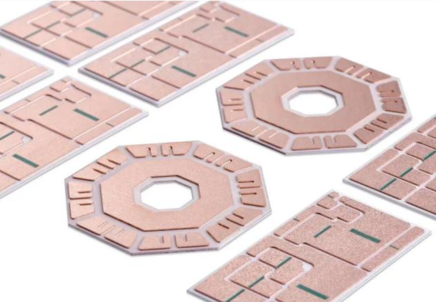
What are the key design rules for DBC/DCB copper patterns (etching, clearance, corners)?
Use wide copper where current is high, avoid sharp corners, keep isolation gaps consistent, and design for manufacturability with realistic line/space. Your layout decisions have a direct impact on thermal uniformity and long-term cycling performance.
How to avoid hotspots and current crowding
- Round internal corners: Sharp corners concentrate current and heat. Rounded corners improve current distribution.
- Use copper pours and neck-down control: Avoid sudden reductions in trace width near die attach or bond areas.
- Plan heat spreading: Add copper area under high-loss components when your mechanical stack allows it.
How to set creepage and clearance for high-voltage areas (practical approach)
Start with your working voltage, transient conditions, and contamination assumptions, then set conservative copper-to-copper gap targets. Use consistent gap geometry across the design so your partial discharge risk does not move around the substrate. If your environment is harsh, treat margin as a design feature, not a luxury.
What are common failure modes in DBC/DCB ceramic substrates, and how do you prevent them?
Most reliability issues trace back to stress concentration, thermal mismatch, or process choices that amplify cycling strain. You can prevent many problems with good geometry, controlled copper thickness choices, and stable assembly methods.
Why delamination happens (and how to reduce risk)
- Stress from cycling: Repeated heating and cooling can load the interface.
- Large copper islands: Very large copper areas can amplify stress in some stacks.
- Prevention ideas: Smooth transitions, balanced copper on both sides when needed, and realistic copper thickness selection.
Why cracks start (and how layout choices help)
- Corner stress: Sharp copper corners can focus stress.
- Mechanical constraints: Overly rigid mounting or uneven torque can add bending.
- Prevention ideas: Radius corners, avoid unnecessary cutouts near high-stress regions, and control mounting flatness.
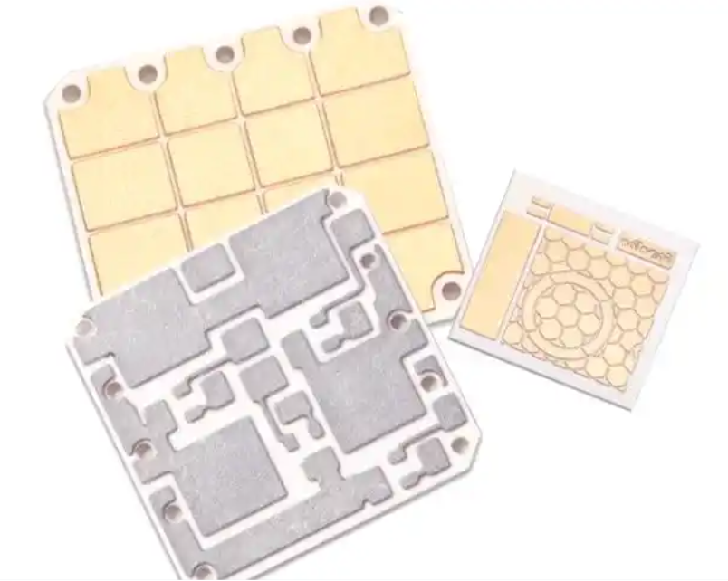
How are DBC/DCB ceramic substrates used in real power semiconductor packages?
They sit between semiconductor chips and the heatsink/baseplate, acting as the insulated thermal highway and the copper circuit at the same time. That is why they are central to power module packaging.
IGBT modules: baseplate, solder, and heat path
In IGBT modules, a DBC/DCB substrate typically supports the die attach layer and wire bonds, then conducts heat through the ceramic down to the baseplate and into the cooling system. The copper pattern also routes phase currents and gate-related connections in a compact, low-inductance layout.
SiC MOSFET modules: faster switching, higher thermal stress
SiC switching can increase thermal and mechanical stress in the stack because designs often push higher power density. This is where ceramic choice, copper thickness strategy, and assembly control become even more important. A stable substrate can protect performance consistency across life-cycle operation.
What information should you send a manufacturer to quote DBC/DCB ceramic substrates fast?
If you want fast quoting and fewer back-and-forth emails, send a complete stack definition plus the copper pattern data and inspection expectations. Power substrates are not “generic PCB,” so clarity saves days.
Include these items in your RFQ package
- 2D drawing (PDF) + dimension tolerances
- Copper pattern files (Gerber or DXF) for top and bottom
- Ceramic type: Al2O3 / AlN / Si3N4
- Ceramic thickness (target + tolerance)
- Copper thickness (top/bottom), single- or double-sided
- Surface finish requirement (example: Ni/Au for bondability)
- Flatness target and any warpage limits
- Reliability goal: thermal cycling expectations and inspection plan
Ask these questions early (they prevent surprises)
- What minimum line/space is realistic for your copper thickness?
- What is your typical etch tolerance window?
- How do you control copper thickness uniformity?
- What inspection data can you provide (thickness, flatness, dielectric checks)?
Why choose EBest as your DBC/DCB ceramic substrates manufacturer?
If you want a supplier that speaks the language of engineers, EBest is built around practical manufacturability, fast feedback, and reliable delivery. We position ourselves as a One-stop PCBA service provider with a strong understanding of power electronics build risks, so your substrate sourcing and downstream assembly stay aligned.
What EBest does differently (engineer-first advantages)
- Free DFM and process adaptation suggestions for copper patterns, clearances, and manufacturable features
- 20 years of manufacturing depth, serving 1800+ customers and 10,000+ engineers
- One-stop support: PCB, components, PCBA, testing, and box-building
- NO MOQ and personal service for prototype and small-volume programs
- Quality systems aligned to regulated and reliability-driven industries (ISO9001, ISO13485, IATF16949, AS9100D)
- MES & Traceability to keep material and process records consistent
- 1.5-week rapid PCBA delivery capability for time-critical projects
- Technical support before and after sales, with prompt feedback (within 12 hours)
- Quick turn-out and on-time delivery mindset
- High quality builds with special request support
What this means for your project
You get clearer manufacturability guidance upfront, fewer drawing revisions, and smoother integration from substrate to assembly. That reduces re-spin risk and keeps your schedule predictable.
FAQ about DBC/DCB ceramic substrates
What is the difference between DBC and DCB substrate?
In most real-world RFQs, they refer to the same copper-on-ceramic concept. Focus on the spec details that change performance: ceramic type, ceramic thickness, copper thickness, surface finish, and reliability requirements.
Which is better for power modules: AlN DBC substrate or Al2O3 DBC substrate?
If you are heat-limited, AlN usually offers a stronger thermal path and can reduce thermal resistance. If your design has enough thermal margin and cost control is critical, Al2O3 is often the best starting point.
Why do Si3N4 DBC substrates show up in automotive and cycling-heavy applications?
Because mechanical toughness and thermal shock resistance can become the limiting factor over long life cycles. When cycling is intense, Si3N4 is often chosen to protect reliability margins.
How do I choose copper thickness for DBC/DCB ceramic substrates?
Start with current level and allowable temperature rise, then choose copper thickness that keeps resistance and hotspots under control. If you also need finer copper features, confirm manufacturable line/space limits early so the copper thickness and pattern can coexist.
What surface finish is common for DBC/DCB ceramic substrates used in power packages?
Ni-based finishes with gold top layers are commonly specified when bondability and stable solderable surfaces matter. The best finish depends on your die attach method, wire bonding approach, and storage/handling needs.
What files do I need to get a fast quote for DBC/DCB ceramic substrates?
Send your 2D drawing, copper pattern data (top/bottom), stack definition (ceramic type + thickness, copper thickness), finish requirement, and any flatness or inspection expectations. Clear input leads to faster quoting and fewer revisions.
Does EBest support prototypes and small-quantity DBC/DCB substrate-related projects?
Yes. We welcome prototype and small-volume programs, and we support fast feedback with Free DFM so your design can move forward with confidence.
Ready to source DBC/DCB ceramic substrates for your power semiconductor packages?
If you need DBC/DCB ceramic substrates for power modules, inverters, IGBT packages, or SiC MOSFET packages, EBest can support your project with engineer-led DFM, responsive quoting, and one-stop manufacturing support. Email us at sales@bestpcbs.com and send your drawing + copper pattern files to start.
You may also like


Tags: DBC ceramic substrate, dbc ceramic substrate manufacturer, dbc substrate for semiconductor, DBC/DCB ceramic substrates, DCB substrate