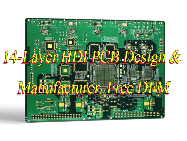
14-Layer HDI PCB solutions are increasingly chosen for designs that demand extreme routing density, stable signal integrity, and compact form factors. As electronic systems move toward higher speeds and smaller footprints, traditional multilayer boards often reach their physical limits. At this point, HDI architecture becomes not an upgrade, but a necessity.
In this article, we will walk through what defines a 14-layer HDI board, how it is structured, how it is manufactured, and how design and fabrication teams can work together to reduce risk. Along the way, we will also discuss real production considerations and explain how an experienced manufacturer can support complex HDI projects from concept to delivery.
What Is A 14-Layer HDI PCB?
A 14-layer HDI PCB is a high-density interconnect circuit board that combines a multilayer structure with advanced interconnection techniques. These techniques mainly include microvias, blind vias, buried vias, and sequential lamination. Unlike conventional 14-layer boards, HDI versions reduce via size and pad dimensions. This creates more usable routing space on each layer. As a result, designers can place finer-pitch components, such as large BGAs and high-pin-count processors, without increasing board size.
In most cases, a 14-layer HDI PCB adopts a multi-step lamination process. Microvias are stacked or staggered to connect adjacent layers. Laser drilling replaces mechanical drilling for these vias, allowing diameters as small as 75–100 µm. Because of this structure, HDI boards are widely used in applications such as networking equipment, medical imaging systems, industrial controllers, and advanced computing platforms
Design Technical Parameters of 14 Layer HDI PCB
Typical specifications for a 14 layer HDI PCB include the following:
| Parameter Category | Typical Specification | Design Consideration |
| Layer count | 14 layers | Often arranged symmetrically |
| Board thickness | 1.6–2.4 mm | Depends on stack-up and materials |
| Minimum line/spacing | 3/3 mil or finer | Impacts routing density |
| Microvia diameter | 75–100 µm | Laser drilled |
| Via types | Blind, buried, stacked, staggered | Chosen by reliability needs |
| Copper thickness | 0.5–1 oz signal, up to 2 oz planes | Balance etching and current |
| Dielectric material | High-Tg FR-4 or low-loss laminate | Selected by signal speed |
| Surface finish | ENIG, ENEPIG, Immersion Silver | Match assembly process |
| Impedance tolerance | ±10% or tighter | Controlled by stack-up |
| Inspection | AOI, X-ray, electrical test | Ensures consistency |
How to Design the Stack-Up for 14-Layer HDI PCB?
14-Layer HDI PCB’s performance hinges heavily on stack-up design. Start with a symmetric structure, as it minimizes board warpage effectively. The 2+10+2 second-order structure is most common here. Outer layers (L1-L2, L13-L14) use laser blind holes, while middle layers (L3-L12) rely on buried holes for interconnection.
Also, divide power and ground layers properly. Allocate 2-3 power layers and 2-4 ground layers for your design. Alternate signal, power, and ground layers to block interference. This layout provides a low-impedance return path and stabilizes high-frequency signals.
Control board thickness within a reasonable range. It usually falls between 0.8-3.2mm, with 1.6mm as the standard option. Stick to this range to keep manufacturing smooth. For inner layers, use RCC (Resin-Coated Copper) material to boost layer adhesion.
Finally, verify the design with simulation tools. Check layer coupling and signal paths beforehand. This step cuts down rework risks and ensures the stack-up fits your actual application needs.

Design Challenges & Solutions for 14 Layers HDI PCB
Below are 5 typical issues and their practical solutions for 14 layers HDI PCB:
- Laser drilling misalignment. It leads to poor layer connectivity and signal loss. Use high-precision exposure machines with ±3mil positioning accuracy. Add alignment marks between layers to correct deviations in real time.
- Uneven micro-hole electroplating. Thin or uneven copper affects conductivity and durability. Adopt ultrasonic stirring during electroplating. Control plating solution parameters to ensure hole copper thickness ≥20μm uniformly.
- Electromagnetic Interference (EMI). Dense wiring raises interference risks for high-frequency signals. Use equal-length differential pair routing (error ≤5mil). Add shielding copper areas around sensitive signal lines to reduce radiation.
- Solder pad peeling in fine-pitch areas. Improper design causes poor adhesion. Optimize pad chamfers and adopt non-linear cutting technology. Clean pad surfaces to avoid oil or impurity residues before processing.
- Board warpage due to unbalanced stress. Asymmetric design or copper distribution triggers deformation. Adopt symmetric stack-up and fill blank areas with grid dummy copper. Keep copper coverage difference between layers <15%.
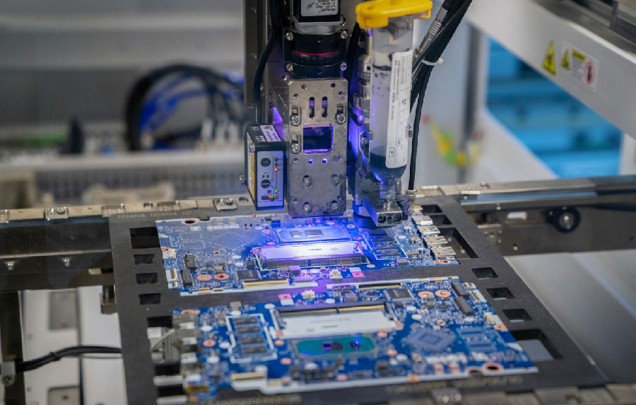
What Are the Manufacturing Processes of 14-Layer HDI PCB?
Below are manufacturing processes of 14-layer HDI PCB:
1. Material Preparation: Select specialized substrates like modified epoxy resin or polyimide for low dielectric constant (Dk~3.0) and high thermal conductivity (0.8W/m·K), paired with ultra-thin copper foil and resin-coated copper (RCC).
2. Inner Layer Fabrication: Coat core laminates with photoresist, expose using laser direct imaging (LDI), develop, and etch to form circuitry. Automated optical inspection (AOI) with 2μm resolution verifies line integrity and detects defects like opens/shorts.
3. Surface Oxidation & Lamination: Treat copper surfaces with oxidation (browning/blackening) to enhance adhesion. Stack cores and prepregs, then apply high-pressure vacuum lamination—repeated 3+ times for 14-layer structures to form sub-composites.
4. Laser Microvia Drilling: Use UV lasers (355nm wavelength) to drill blind microvias (50–100μm diameter) with 5μm spot precision. Depth control ensures connections only between adjacent layers.
5. Via Metallization: Deposit electroless copper (0.3–1μm) on via walls, followed by electroplating to fill vias completely, copper paste filling may be used for thermal-critical designs (8–10W/m·K conductivity).
6. Outer Layer Patterning: Apply semi-additive process (SAP): deposit thin copper, pattern with photoresist/LDI, electroplate traces (5–10μm), then etch excess copper to achieve ultra-fine lines (≤0.05mm).
7. Through-Hole (PTH) Drilling & Plating: Mechanically drill plated through-holes (PTHs) for inter-layer connectivity. Desmear holes, then perform electroless copper deposition and panel electroplating for conductivity.
8. Solder Mask & Surface Finish: Apply liquid photoimageable solder mask (LPI), expose/develop to expose pads, then add surface treatment (e.g., ENIG, OSP) for solderability and corrosion resistance.
9. Electrical & Reliability Testing: Conduct AOI for outer layers, X-ray inspection for microvia fill quality, flying probe/ICT for electrical continuity, and thermal stress tests to validate reliability.
10. Routing & Final QA: CNC-rout board outlines, perform microsection analysis for process validation, and conduct final dimensional/visual inspection before packaging.
Why Choose EBest(Best Technology) for 14-Layer HDI PCB Manufacturer?
Reasons why choose EBest(Best Technology) for 14-layer HDI PCB manufacturer:
- Free DFM Analysis: We conduct full-dimensional design reviews upfront. Identify compatibility issues between design and production early, optimize routing and stack-up, cut rework times and project cycles, and ensure smooth mass production.
- 19 Years of HDI PCB Experience: We deeply understand process pain points across diverse application scenarios. Respond quickly to special requirements with mature solutions, ensuring stable project progress without repeated adjustments.
- Strong Process Capabilities: We specialize in high-layer count HDI PCB production. Combined with advanced processes like mSAP, it fits high-density and high-frequency demands, offering sufficient space for complex designs.
- Strict Quality Control & Certified Assurance: We hold ISO9001, AS9100D and IATF 16949 certifications. These cover consumer, aerospace and automotive electronics standards. Every batch goes through 19 strict inspections for traceable quality.
- Expedited Production & 24-Hour Prototyping: Get 14-Layer HDI PCB prototypes in 24 hours. Urgent mass production delivers in 3 days at the earliest, accelerating R&D iterations and product launch schedules.
- One-Stop PCBA Services: Integrate PCB manufacturing, component sourcing, SMT assembly and function testing. Reduce multi-supplier communication costs for seamless connection from design to finished products.
- Traceable Production Data with MES System: Our MES system monitors the entire production process. Track every detail from raw materials to finished products, ensuring full transparency and quality accountability.
Our HDI PCB Manufacturing Capabilities
| Item | Capabilities |
| Layer Count | 1 – 32 Layers |
| Max Board Dimension | 2424″ (610610mm) |
| Min Board Thickness | 0.15mm |
| Max Board Thickness | 6.0mm – 8.0mm |
| Copper Thickness | Outer Layer: 1oz~30oz, Inner Layer: 0.5oz~30oz |
| Min Line Width/Line Space | Normal: 4/4mil (0.10mm); HDI: 3/3mil (0.076mm) |
| Min Hole Diameter | Normal: 8mil (0.20mm); HDI: 4mil (0.10mm) |
| Min Punch Hole Dia | 0.1″ (2.5mm) |
| Min Hole Spacing | 12mil (0.3mm) |
| Min PAD Ring(Single) | 3mil (0.075mm) |
| PTH Wall Thickness | Normal: 0.59mil (15um); HDI: 0.48mil (12um) |
| Min Solder PAD Dia | Normal: 14mil (0.35mm); HDI: 10mil (0.25mm) |
| Min Soldermask Bridge | Normal: 8mil (0.2mm); HDI: 6mil (0.15mm) |
| Min BAG PAD Margin | 5mil (0.125mm) |
| PTH/NPTH Dia Tolerance | PTH: ±3mil (0.075mm); NPTH: ±2mil (0.05mm) |
| Hole Position Deviation | ±2mil (0.05mm) |
| Outline Tolerance | CNC: ±6mil (0.15mm); Die Punch: ±4mil (0.1mm); Precision Die: ±2mil (0.05mm) |
| Impedance Controlled | Value>50ohm: ±10%; Value≤50ohm: ±5ohm |
| Max Aspect Ratio | 0.334027778 |
| Surface Treatment | ENIG, Flash Gold, Hard Gold Finger, Gold Plating(50mil), Gold finger, Selected Gold plating, ENEPIG, ENIPIG; HAL, HASL(LF), OSP, Silver Immersion, Tin Immersion |
| Soldermask Color | Green/White/Black/Yellow/Blue/Red |
Case Studies of Our 14 Layers HDI PCB Board
Project Background: The client needed a solution for AI servers used in large-scale data training. A compact PCB with high-speed signal transmission and efficient heat dissipation was required, which traditional PCBs couldn’t fulfill. They chose our 14-Layer HDI PCB with mSAP process.
Project Requirements: Support 40GHz+ signal transmission (insertion loss ≤0.5dB/inch), ±5% impedance precision (for 50Ω/75Ω differential signals), 105℃ long-term working temperature resistance, and over 99% mass production yield.
Core Challenges:
- High-frequency signal attenuation and crosstalk from 14-layer dense wiring.
- Board deformation due to uneven GPU cluster heat distribution.
- 3. ±3mil alignment accuracy for 0.076mm micro blind holes.
Our Solutions:
- Optimized 2+10+2 symmetric stack-up via free DFM, with 3 ground layers and equal-length differential routing (≤5mil error) to reduce crosstalk.
- Adopted FR-4 high Tg (180℃) material, embedded copper layers and 40 thermal vias/cm² for heat dissipation.
- Used LPKF laser drills and MES system to ensure blind hole precision.
Output Results: The 14-Layer HDI PCB achieved 40GHz transmission with 0.45dB/inch insertion loss, boosting signal stability by 30%. Working temperature dropped to 78℃ under full GPU load. Mass production yield hit 99.2%, and the product was batch-deployed in global AI data centers.
How to Get A Quote for Your HDI PCB Project?
Steps to Get A Quote for Your HDI PCB Project:
1. Prepare Complete Design Files: Submit Gerber files, BOM (Bill of Materials), layer stack-up details, and any specific requirements (e.g., impedance control, via types) to ensure accurate cost estimation.
2. Specify Material & Surface Finish: Clearly state dielectric material (e.g., high-Tg FR-4, low-loss laminate), copper thickness, and surface finish (e.g., ENIG, Immersion Silver) to match signal integrity and assembly needs.
3. Define Technical Parameters: Include minimum line/space width (e.g., 3/3 mil), microvia diameter (75–100 µm), board thickness (1.6–2.4 mm), and impedance tolerance (±10% or tighter) for precise manufacturing planning.
4. Select PCB Suppliers: Shortlist suppliers with HDI expertise, check their capabilities (e.g., laser drilling for microvias, stack-up optimization), and verify quality certifications (e.g., ISO, ITAR).
5. Request Detailed Quotes: Contact suppliers with your specifications, ask for itemized quotes (material, labor, tooling, testing), and clarify turnaround time (prototype vs. mass production).
6. Compare Quotes & Validate: Evaluate quotes based on cost, lead time, and supplier reputation; request samples or case studies for verification; ensure compliance with inspection standards (AOI, X-ray, electrical test).
Welcome to contact us if you have any request for HDI PCB design, prototyping, mass production and assembly: sales@bestpcbs.com.