

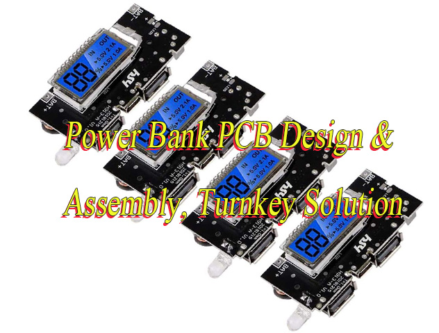
How to design a power bank PCB? This blog is mainly about working principle, circuit diagram, design guide, production and assembly process for power bank circuit board.
Are you struggling with these questions?
- What to do when design verification requires repeated modifications, causing delays in time to market?
- How to balance cost and performance when low-cost solutions raise quality concerns and high-end options exceed budget?
- How to overcome coordination challenges in assembly from PCB to casing/battery integration?
As a professional power bank PCB manufacturer, EBest Circuit (Best Technology) can provide you service and solutions:
- Free DFM (Design for Manufacturability) analysis: Identify potential issues in trace width, via design, and impedance control at the design stage to prevent rework and reduce validation cycles by over 30%.
- Cost-sensitive design solutions: Leveraging 19 years of specialized Power Bank PCB experience, we utilize cost-effective FR4 substrates combined with microvia technology to reduce BOM costs by 15-20% while maintaining 200W fast-charging thermal performance.
- One-stop assembly services: Covering the full process from PCB SMT/through-hole assembly to casing integration and functional testing, ensuring over 99.2% on-time delivery rates and eliminating multi-supplier coordination costs.
Welcome to contact us if you have any request for power bank PCB: sales@bestpcbs.com.
What Is a Power Bank Circuit Board?
A power bank circuit board( also called as power bank PCB) is an integrated platform that connects the battery cell, power path modules, USB interfaces, and safety components into one compact structure. It governs how the battery stores and releases energy. Even more, it stabilizes voltage output and prevents faults during charging or discharging.
Typically, a power bank uses a lithium-ion or lithium-polymer cell. This means the PCB must maintain precise control of current flow. As the board handles sensitive energy levels, the layout must keep copper resistance low while guiding heat away from active areas.
Furthermore, many power banks now support dual-port or triple-port fast charging. This requires higher current handling, intelligent power distribution, and extra sensors to manage temperature. A well-structured PCB helps balance all these needs without expanding size.
How Does a Power Bank Circuit Work?
1. Electric Energy Storage: Lithium-ion or lithium-polymer batteries serve as energy storage units, converting external electrical energy into chemical energy during charging. Typical voltage ranges are 3.7-4.2V, offering high energy density and long cycle life.
2. Charging Management: Charging management chips like TP4056 enable constant current/constant voltage charging. They convert standard 5V USB input to approximately 4.2V for battery charging while integrating overcharge protection and current limiting to ensure safe charging.
3. Battery Protection: Dedicated protection ICs such as DW01 monitor battery voltage, current, and temperature. They automatically disconnect the circuit during over-discharge (voltage <2.5V), overcharge (voltage >4.3V), short circuits, or over-temperature conditions to prevent damage and safety hazards.
4. Boost Output: DC-DC boost circuits, such as those based on the MT3608 Boost topology, elevate the battery’s 3.7-4.2V voltage to a stable 5V output. This meets USB device charging requirements with conversion efficiency of 85%-92% and supports output currents of 1A/2A/2.4A.
5. Output Control and Detection: Microcontrollers (MCUs) or power management ICs handle smart device recognition, output activation/deactivation, and integrate user interaction features like battery level display (LED/digital), flashlight control, and charging status indicators.
6. Auxiliary Circuits: Includes LED indicator circuits (battery/status display), button switch circuits (manual function control), temperature sensors (monitoring battery/circuit temperature), and over-voltage/over-current protection modules to enhance user experience and system safety.
Power Bank PCB Circuit Diagram Sample
A typical power bank PCB circuit diagram contains several core blocks:
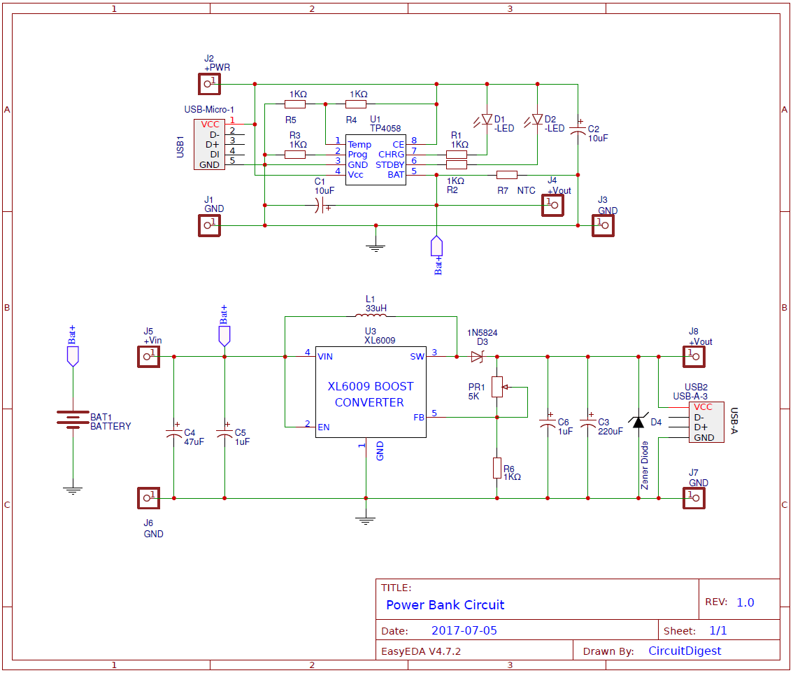
At a glance, you will see the following sections:
- Battery Protection Module: Includes overcharge, over-discharge, short-circuit, and temperature control.
- Charging Controller: Handles input regulation, USB-C PD negotiation, and constant-current/constant-voltage behavior.
- Boost & Buck Converters: Adjust battery voltage to USB output levels, typically 5V, 9V, or 12V.
- Load Detection Circuit: Activates output only when a device is connected.
- USB Ports and Connectors: May include USB-A, USB-C, micro-USB, or lightning ports.
- Current Sense Resistors: Track real-time current flow for protection and monitoring.
- LED or LCD Module: Shows remaining battery level.
These modules form the backbone of the circuit, working together to manage energy with precision.
How to Design A Power Bank PCB?
Below Is A Detailed Power Bank PCB Design Guide for Your Reference:
1. Define Design Requirements and Specifications
- Determine total capacity (e.g., 5000mAh, 10000mAh), input/output voltage (e.g., 5V/2A, 9V/2A fast charging), and charging protocol compatibility (e.g., PD, QC).
- Specify physical dimensions based on product form factor (e.g., card-style, cylindrical) and define PCB size, thickness, and interface positions (USB-A/C, Lightning).
- Ensure compliance with international certifications (e.g., CE, FCC, UL) and battery safety standards (e.g., UN38.3), including overcharge, over-discharge, and short-circuit protection.
2. Core Circuit Module Design
- Select dedicated BMS chips (e.g., TI, Maxim, ADI) integrating cell balancing, temperature monitoring, and capacity calculation.
- Design constant-current/constant-voltage charging circuits supporting multi-mode charging (e.g., solar input, Type-C PD input) with reverse-current protection.
- Implement output control modules using DC-DC converters (e.g., boost/buck circuits) for stable output and multi-protocol fast-charging recognition (e.g., PD3.0, SCP).
3. Component Selection and Layout Optimization
- Choose lithium-ion/lithium-polymer cells based on capacity, discharge rate, and cycle life, prioritizing reputable brands (e.g., Samsung, Panasonic, CATL).
- Cluster heat-generating components (e.g., MOSFETs, DC-DC chips) with heat sinks or thermal pads; keep sensitive components (e.g., op-amps) away from high-frequency noise sources.
- Use short, thick power traces to reduce impedance; employ differential routing for high-speed signals. Plan multi-layer PCB layering (signal, power, ground planes) for effective grounding.
4. Protection and Safety Mechanisms
- Integrate multi-level protection circuits including over-voltage protection (OVP), over-current protection (OCP), over-temperature protection (OTP), and short-circuit protection (SCP) with redundant backups (e.g., dual fuses).
- Add thermal insulation between cells and PCB to prevent thermal runaway; use flame-retardant PCB substrates (e.g., FR-4) and apply conformal coating in critical areas.
- Design status indicators (e.g., LED charge level), NFC modules, or Bluetooth modules for battery monitoring/firmware updates to enhance user experience.
5. Thermal Management and EMC Design
- Conduct thermal simulation to determine heat dissipation paths; add thermal copper, vias, or thermal adhesive to heat-generating components. Incorporate fans or heat sinks if necessary.
- Implement EMC/EMI countermeasures by adding filter capacitors and common-mode chokes at power entry points and high-speed signal lines. Follow the 3W principle (minimum spacing) to minimize crosstalk.
- Shield sensitive circuits (e.g., MCUs, ADCs) with metal enclosures; adopt star grounding to avoid ground loop noise.
6. Prototype Verification and Testing
- Validate charging/discharging efficiency, fast-charging protocol compatibility, and accuracy of charge level displays. Ensure all protection functions trigger correctly.
- Conduct reliability tests including thermal cycling, vibration/shock, and salt spray tests to verify stability under extreme conditions.
- Perform EMC compliance tests (e.g., CISPR 22 for conducted/radiated emissions, ESD testing) to meet international standards.
7. Cost Optimization and Design for Manufacturing (DFM)
- Standardize components with common packages (e.g., SOP, QFN) to reduce customization; adopt multi-sourcing strategies to mitigate procurement risks.
- Optimize PCB processes by selecting appropriate board thickness, copper thickness, and surface finishes (e.g., HASL, ENIG) to balance cost and performance. Use panelization to improve production efficiency.
- Incorporate Design for Testability (DFT) with test points at critical nodes for post-repair and quality checks; include programming interfaces (e.g., SWD) for firmware updates.
8. Documentation and Traceability
- Provide detailed technical documentation including schematics, PCB layouts, BOM lists, and test reports to ensure design reproducibility. Document design change history for future iterations.
- Establish a component traceability system to ensure reliable sourcing of critical materials (e.g., cells, chips); collaborate closely with manufacturers to optimize production processes.
- Create clear user manuals with charging/discharging guidelines and safety warnings; label PCBs with version numbers, production dates, and safety certification marks.
How to Make a Power Bank PCB?
Below Are Power Bank PCB Manufacturing Processes:
1. Substrate Material Cutting and Pre-treatment
- Substrate Selection: Choose FR-4 for consumer-grade, aluminum substrate for high-heat scenarios, or high-frequency materials (e.g., Rogers 4350B for RF modules) with cutting precision ±0.1mm.
- Surface Cleaning: Use plasma or chemical cleaning to remove oxidation and contaminants for strong adhesion.
- Brown Oxidation Treatment: Micro-etch copper foil to increase surface roughness and enhance interlayer bonding strength.
2. Inner Layer Circuit Pattern Transfer
- Dry Film Lamination: Apply photosensitive dry film evenly on the substrate, ensuring no bubbles or wrinkles via hot roller press.
- Exposure and Development: Use LDI (Laser Direct Imaging) or traditional film exposure, with line width/spacing precision ±5μm after development.
- Etching Process: Remove unprotected copper with alkaline etchant, followed by micro-etching to eliminate copper residue.
3. Multilaminate Pressing and Layer Alignment
- Prepreg Laying: Apply prepreg sheets (PP sheets) between inner layers, controlling resin content and flow for strong interlayer bonding.
- Vacuum Lamination: Press under vacuum at 180-200°C and 300-500psi to ensure void-free, delamination-free layers.
- X-ray Drilling Alignment: Align layers precisely via X-ray drilling of registration holes for subsequent drilling accuracy.
4. Mechanical Drilling and Plating
- CNC Drilling: Drill holes (0.1-1.0mm diameter) with positional accuracy ±0.05mm and wall roughness ≤20μm.
- Copper Electroplating: Deposit conductive layer (≥0.02mm) via electroless copper, then thicken to 0.03-0.05mm by electroplating for reliable conductivity.
- Hole Wall Treatment: Remove drilling residue via desmear process, and enhance bonding via chemical plating.
5. Outer Layer Circuit Pattern Creation
- Outer Layer Dry Film Lamination: Repeat exposure-development process on outer substrate to form circuit patterns.
- Pattern Plating: Electroplate lines to ≥35μm copper thickness for high current capacity.
- Etching and Stripping: Remove copper outside dry film protection to finalize outer circuit.
6. Surface Treatment and Solder Mask
- Solder Mask Coating: Apply solder mask ink (20-30μm thickness) via screen printing or spraying to cover non-pad areas.
- Character Printing: Mark component symbols and version numbers via screen printing or laser printing.
- Surface Finish: Apply ENIG, OSP, or HASL based on requirements to enhance solderability and oxidation resistance.
7. Final Testing and Reliability Validation
- Electrical Testing: Verify conductivity, insulation resistance (≥100MΩ), and shorts/opens via flying probe or fixture testing.
- AOI Inspection: Detect defects (e.g., gaps, burrs) via automated optical inspection for visual quality control.
- Reliability Testing: Conduct high-temperature aging (85°C/85%RH/168h), thermal cycling (-40°C~125°C/100 cycles), and vibration tests (per IEC 68-2-6) for long-term reliability.

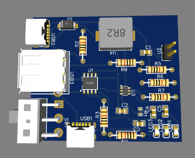
Power Bank PCB Assembly Process
Below Are Power Bank PCB Assembly Process:
1. PCB Inspection & Preparation
- Verify PCB meets IEC 62368-1 safety standards and IPC-6012 Class 2 quality requirements.
- Conduct 100% visual inspection for defects (e.g., solder masks, pad alignment).
2. Component Sourcing & IQC
- Source Grade-A lithium-ion/polymer cells, USB ports, capacitors, and protection ICs.
- Perform incoming quality control (IQC): test battery capacity (≥95% nominal), internal resistance, and component functionality.
3. SMT Assembly
- Use SMT machines to mount surface-mount devices (SMDs: resistors, capacitors, ICs) onto PCB pads.
- Execute reflow soldering at 230–250°C to fix components permanently.
4. Through-Hole Component Installation
- Manually insert through-hole components (e.g., connectors, switches) into PCB holes.
- Apply wave soldering or selective soldering for reliable electrical connections.
5. Battery Pack Integration
- Connect battery cells in parallel/series using nickel strips or laser-welded joints.
- Attach battery terminals to PCB pads via spot welding or soldering, ensuring polarity accuracy.
6. Functional Testing
- Conduct charge/discharge cycle tests (3–5 cycles) to validate performance and safety.
- Test parameters: input/output voltage (5V±0.25V), current stability, overcharge/overdischarge protection.
7. Final Assembly
- Assemble PCB, battery pack, and housing using screws/adhesives.
- Route cables internally to avoid external damage; secure with zip ties or adhesive pads.
8. Certification & Compliance
- Ensure compliance with UN38.3 (transport safety), CE (EMC/LVD), and UL 2056 (US safety).
- Apply region-specific labels (e.g., RCM for Australia, KC for South Korea).
9. Packaging & Logistics
- Package in ESD-safe materials with user manuals and warranty cards.
- Attach certification stickers (e.g., FCC, RoHS) for international shipping.
Why Choose EBest Circuit (Best Technology) as Power Bank PCB Manufacturer?
Reasons Why Choose EBest Circuit (Best Technology) As Power Bank PCB Manufacturer:
- Precise Cost Control and Customized Solutions: Leveraging 19 years of specialized Power Bank PCB manufacturing expertise, we deliver cost-sensitive designs through optimized material selection and process refinement. For instance, adopting high-cost-performance FR4 substrates with microvia technology reduces BOM costs by 15-20% compared to conventional solutions, while free DFM analysis preemptively identifies design flaws to minimize rework expenses for overseas clients.
- Rapid Prototyping System: Emergency orders benefit from a 24-hour rapid sampling channel paired with real-time remote design review platforms. This system has enabled European clients to compress development cycles for fast-charging Power Banks from the industry average of 28 days to just 14 days, accelerating time-to-market.
- Strict Quality Control System: Bulk orders undergo 100% AOI optical inspection and electrical performance testing, adhering to IATF 16949 automotive-grade process standards. A case study for a North American client demonstrated 0 return rates across 5,000 Power Bank PCBs, with critical parameters like voltage resistance and impedance fluctuation controlled within ±3%.
- International Compliance Certification Portfolio: Certifications including ISO 9001, IATF 16949, medical-grade ISO 13485, and RoHS 2.0 cover multi-scenario applications from consumer electronics to medical devices. Medical certification, for example, allowed a German client to directly enter the EU medical device market, saving approximately €80,000 in additional certification costs.
- Experience-Driven DFM Value-Added Services: Free DFM reports provide manufacturability scoring, defect warnings, and optimization recommendations. Historical data shows that optimizing trace spacing and via designs for a U.S. client reduced rework rates by 30%, saving over $200,000 in annual maintenance costs.
- High-Power Density Process Innovation: High-Tg substrates combined with blind/buried via technology support 200W+ fast-charging power density in Power Bank PCBs. Testing confirms a 30% improvement in heat dissipation efficiency versus traditional designs, meeting EU ERP energy standards and lowering product certification barriers for international clients.
- Flexible Capacity and Small-Batch Support: Scalable production lines accommodate seamless transitions from 10-piece samples to million-unit volumes, ideal for overseas clients’ NPI phases. Modular production configurations enable 48-hour rapid turnaround for small batches, eliminating idle capacity costs.
- Global Engineering Collaboration Network: A multilingual senior engineering team provides 7×12 technical support via cloud-based design platforms. A 48-hour EMC troubleshooting resolution for a Japanese client prevented project delays, showcasing responsive cross-border collaboration capabilities.
Case Studies of Our Power Bank PCB Board
Project Background
- The client is a brand specializing in consumer electronics and plans to launch a cost-effective, fast-charging portable power bank. The product targets overseas markets, requiring compact design while achieving high-efficiency charging/discharging and complying with international safety and energy efficiency standards.
Client Requirements
- Output power ≥10 W (5 V/2 A) with support for mainstream fast-charging protocols (e.g., QC3.0).
- Overall charging efficiency >90% to extend battery usage time.
- PCB size controlled within 50 mm × 30 mm for portable enclosure design.
- Complete delivery of PCB and PCBA designs (including schematics, layout, hardware, and software).
Challenges
- Space Constraints: Arranging high-current paths, filter capacitors, and thermal copper foils within limited area while maintaining low EMI.
- Thermal Management: Significant temperature rise in switching components during 2 A continuous output, requiring layout and copper pour optimization to reduce hotspot temperatures.
- Signal Integrity: High-frequency switching noise prone to interfering with voltage feedback loops, affecting output stability.
- Cost-Efficiency Balance: Meeting >90% energy efficiency target while controlling BOM costs.
Solutions
Architecture Selection
- Adopt integrated synchronous rectification buck-boost IC (e.g., Injoinic IP5328P) to reduce peripheral components and enhance conversion efficiency.
- Built-in intelligent battery management and multi-protocol fast-charging recognition to meet compatibility requirements.
PCB Layout Optimization
- Power Path: Place input/output filter capacitors close to IC pins and position switching transistors and inductors nearby to shorten high-frequency loops.
- Ground Plane Design: Implement a complete ground plane in 4-layer PCB structure for low-impedance return paths and EMI suppression.
- Thermal Design: Widen high-current traces to ≥0.3 mm and add thermal vias under power components to dissipate heat to the ground plane.
- Zoning Layout: Separate analog control circuits from switching power supplies to prevent noise coupling.
Simulation and Verification
- Validate voltage drop and noise compliance under full load via power integrity simulation.
- Confirm key component temperature rise ≤40 K through thermal simulation to ensure long-term reliability.
Results
- Performance Metrics: Actual measured efficiency of 92% (5 V/2 A output), support for QC3.0/PD and other fast-charging protocols, output ripple <50 mV.
- Size and Delivery: PCB size 48 mm × 28 mm, full design files provided (schematics, PCB, BOM, and assembly drawings).
- Client Value: First-pass production success, CE/FCC certification achieved, mass shipments to European and American markets, with customer feedback confirming expected battery life and charging speed.
How Much Does A Power Bank PCB Board Cost?
The price of a typical power bank PCB (excluding battery) is usually between $5 and $20, depending on several factors. For example, the unit price of a basic double-layer FR-4 PCB can be as low as $0.5-$1 when ordering in small batches (around 10 pieces), while a dedicated power bank motherboard with Type-C, dual USB ports, and charging management functions can reach $19 per piece.
Key factors affecting the price include: the number of PCB layers (2 layers are cheaper than 4 layers), the type of board material (FR-4, metal-based or flexible boards have different costs), the size and complexity (the higher the line width, impedance control, and component density, the higher the price), the surface treatment process, such as gold plating, tin plating, etc., the order quantity(large batches significantly reduce the unit price), and whether it includes additional functions, such as fast charging protocols, battery protection circuits. Therefore, the actual price needs to be determined based on the specific specifications and purchase quantity.
Conclusion
In conclusion, that’s all about power bank PCB’s working principle, circuit diagram, design guide, production and assembly process. If you need any help for power bank PCB, please feel free to contact us: sales@bestpcbs.com.
You may also like


Tags: power bank circuit board, power bank PCB, power bank PCB assembly, Power Bank PCB Circuit Diagram, power bank PCB design, power bank PCB price