

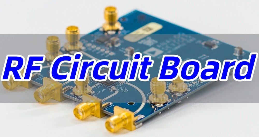
An RF circuit board is a specialized printed circuit board designed to operate at radio frequencies, typically from around 100 MHz up to about 2 GHz, where signal integrity and controlled impedance are paramount. Above this range, designs are usually classified as microwave PCBs, which follow similar principles but face even tighter constraints on materials, layout, and loss control. This guide will walk you through the critical considerations—from materials and design to supplier selection—for choosing the right RF PCB for your application.
Selecting the right RF circuit board is a complex challenge that can make or break the performance of wireless modules, communication systems, and radar equipment. Common frustrations include:
- Unexpected Signal Degradation: High-frequency signals are susceptible to loss and interference, leading to poor performance.
- Impedance Control Challenges: Achieving and maintaining a consistent characteristic impedance (e.g., 50Ω) is difficult but critical for signal integrity.
- Material Selection Confusion: Choosing the wrong RF PCB material can result in inefficient thermal management and unacceptable dielectric losses.
- Complex Design and Layout: RF PCB design requires specialized knowledge; a small routing error can severely impact functionality.
- Finding a Reliable Manufacturing Partner: Many standard PCB manufacturers lack the expertise and equipment to reliably produce high-quality microwave PCBs.
Overcoming these challenges is possible with a clear understanding of RF fundamentals and a partnership with an experienced RF printed circuit boards supplier. The solutions directly address these pain points:
- Superior Materials: Utilizing low-loss laminate materials with stable dielectric constants to minimize signal degradation.
- Precision Engineering: Employing advanced design and fabrication techniques to ensure tight impedance control and consistent performance.
- Expert Material Guidance: Providing recommendations on specialized materials like PTFE or ceramic-filled laminates for optimal thermal and electrical properties.
- Adherence to Strict Design Rules: Following established RF PCB design guidelines to avoid common layout pitfalls.
- Partnering with a Specialized Supplier: Choosing a manufacturer like EBest Circuit (Best Technology), which specializes in RF and microwave printed circuit boards, ensures access to the necessary expertise and quality controls.
At EBest Circuit (Best Technology), we are a specialized manufacturer of high-frequency circuit boards. With 19 years of extensive experience in advanced materials and precise fabrication processes, we are committed to delivering RF circuit boards that meet the most demanding electrical specifications. Pls feel free to contact us at sales@bestpcbs.com to discuss your RF circuit boards project requirements.
What Is an RF Circuit Board?
An RF (Radio Frequency) circuit board is engineered to transmit, receive, and process high-frequency signals typically ranging from hundreds of megahertz (around 100 MHz) up to approximately 2 GHz. Unlike standard PCBs used for low-frequency electronics, the performance of an RF circuit board is highly sensitive to its physical properties—including dielectric constant, layer stack-up, trace geometry, and impedance control—which must be precisely managed to ensure stable, low-loss signal propagation.
- Core Function:
The primary role of an RF PCB is to guide RF signals with minimal loss, distortion, or radiation.
This is crucial in applications like smartphones, GPS units, and wireless networking equipment. - Key Characteristics:
These boards are defined by controlled impedance traces, specific material selection, and specialized structures like ground planes and shielding to contain electromagnetic fields.
Proper RF circuit board design is fundamental to their operation.
In summary, an RF circuit board is a high-performance platform where the board itself is an integral component of the circuit’s functionality.
What Is the RF Circuit Board Material?
The choice of material is arguably the most critical decision in RF PCB design. Standard FR-4 is often insufficient for high frequencies due to its high loss tangent and unstable dielectric constant.
- Low Loss Tangent (Df): Materials with a low dissipation factor (Df) are essential to minimize energy loss converted into heat. Common options include PTFE (Teflon), ceramic-filled PTFE composites (e.g., Rogers RO4000® series), and hydrocarbon ceramics.
- Stable Dielectric Constant (Dk): A stable dielectric constant (Dk) across frequency and temperature is vital for predictable impedance and phase response.
- Thermal Management: High-frequency circuits can generate heat, so materials with good thermal conductivity (e.g., ceramic-filled laminates) are often preferred.
- Common Materials: Popular RF PCB material choices are Rogers RO4350B (a balance of performance and cost), PTFE-based materials for extreme high-frequency applications, and specialized China PTFE laminate circuit boards for RF and microwave industries.
Selecting the right RF circuit board material ensures signal integrity, thermal stability, and overall reliability, forming the foundation of a successful RF PCB project.
What Are the Differences Between RF and Microwave Printed Circuit Board?
The terms “RF” and “microwave” are often used interchangeably, but there is a technical distinction that influences design and material choices.
- Frequency Range:
While the broader radio frequency spectrum spans from kilohertz up to hundreds of gigahertz, in PCB engineering practice RF PCBs usually refer to boards operating in the ~100 MHz to 2 GHz range, and microwave PCBs to those above 2 GHz.
As frequency increases, wavelengths shorten, and the circuit board’s physical dimensions become a more critical part of the circuit. - Design Complexity:
Microwave PCB design often deals with transmission line effects, wave propagation, and parasitic effects that are less pronounced at lower RF frequencies.
This requires more sophisticated modeling and simulation. - Material Requirements:
While both require low-loss materials, microwave PCBs demand materials with exceptionally stable Dk and ultra-low loss tangents, such as pure PTFE, to function effectively at these higher frequencies.
In practice, the design principles for RF and microwave printed circuit board are similar, but microwave applications push the requirements for precision and material performance to a greater extreme.
What Parts of a Circuit Board Confine RF Transmission Signals?
Containing RF energy within designated pathways is essential to prevent interference and signal loss. Key structures achieve this confinement.
- Controlled Impedance Transmission Lines: Microstrips and striplines are the primary conduits. A consistent cross-section and proximity to a ground plane create a controlled electromagnetic field around the trace.
- Ground Planes: A solid, unbroken ground plane beneath signal layers is critical. It provides a return path for the signal and helps contain the electromagnetic field.
- Shielding: Circuit board RF shielding, often in the form of metal cans or fences soldered to the board, physically isolates sensitive RF sections like amplifiers or oscillators from radiating or receiving interference.
- Vias: A “via fence” or a row of grounding vias around a microstrip line can act as a barrier, further confining the signal and reducing coupling to adjacent circuits.
Proper RF PCB routing and the use of these structures are fundamental to ensuring signals travel only where intended.
What Is a Radio RF Pass-Through Circuit Board?
An RF pass-through, or feedthrough, is a specialized circuit board feature designed to allow an RF signal to pass from one environment to another—for example, from the interior of a shielded enclosure to an external antenna—with minimal signal degradation.
- Function: It replaces a coaxial cable connector in space-constrained applications, providing a more integrated and reliable connection. It typically uses a controlled impedance transmission line that passes through the board edge or a cutout.
- Construction: It often involves a circuit board mount antenna connector RF coax header or a carefully designed trace that transitions the signal. The key is maintaining impedance continuity at the transition point to prevent reflections.
This component is vital for compact wireless devices where a standard connector is not feasible.
How to Identify an RF Antenna on a Circuit Board?
Identifying an RF antenna is a key skill for debugging or reverse-engineering. Here’s how to identify an RF antenna on a circuit board:
- Physical Shape: Antennas are often distinct geometric shapes—a meandered trace, a zig-zag pattern, a circular loop, or a simple straight trace—typically located on the board’s periphery.
- Connection Point: The antenna trace will usually connect to a single component, such as an RF transceiver chip or a RF module, via a matching network (small capacitors and inductors).
- Lack of Connections: Unlike other traces, the antenna trace will be isolated and not connected to a dense network of other components.
- Associated Components: Look for a circuit board mount antenna connector RF or a dedicated IC near the antenna for signal processing.
In an x10 motion detector circuit board RF antenna, for instance, you would typically find a simple, quarter-wave trace along the edge of the board.
What Is a Coupon in an RF Circuit Board?
A coupon, or test coupon, is a dedicated section included in the panel of an RF circuit board that is fabricated simultaneously with the main board but is intended for testing, not for functional use.
- Purpose: It allows the manufacturer and the designer to verify that the fabrication process meets specifications without damaging the actual product board. Tests performed on coupons include:
- Impedance Verification: Measuring the actual characteristic impedance of a trace.
- Plating Quality: Checking the thickness and uniformity of copper plating.
- Layer-to-Layer Registration: Ensuring all layers are aligned correctly.
Using a coupon is a best practice in practical RF printed circuit board design as it provides objective data on the board’s quality.
How to Do RF Circuit Board Design?
Successful RF circuit board design requires meticulous planning and adherence to specific guidelines, often detailed in an RF PCB design guidelines pdf.
- Plan the Stack-up: Define the layer stack-up early, ensuring symmetrical construction and dedicated ground planes to control impedance and provide shielding.
- Control Impedance from the Start: Use a PCB field solver tool to calculate the correct trace width for your target impedance (e.g., 50Ω) based on your chosen material’s dielectric thickness and constant.
- Mindful Component Placement: Group RF components closely to minimize trace lengths. Isolate noisy digital sections from sensitive analog/RF sections.
- Implement Careful RF PCB Routing:
- Keep RF traces short, straight, and wide enough for the target impedance.
- Avoid 90-degree bends; use 45-degree angles or curved bends.
- Provide generous spacing between RF traces and other signals.
- Use a Continuous Ground Plane: Do not route other signals on the ground plane layer; splits or cutouts can ruin performance.
- Incorporate Proper Shielding and Vias: Use ground vias generously, especially around RF traces, to suppress unwanted modes and provide shielding.
Following these steps is essential for creating a functional RF amplifier circuit board or any other high-frequency circuit.
How to Evaluate RF Printed Circuit Boards Supplier?
Choosing the right RF printed circuit boards supplier is as critical as the design itself. Key evaluation criteria include:
- Technical Expertise: Do they understand RF microwave circuit board design principles? Can they provide feedback on your stack-up and material choices?
- Manufacturing Capability: Do they have the equipment for controlled impedance testing, laser drilling of small vias, and tight tolerance etching?
- Material Experience: Do they stock or have easy access to a wide range of specialized RF circuit board materials?
- Quality Control: What is their process for testing impedance, electrical continuity, and quality? Do they provide test coupons and data?
- Proven Track Record: Ask for examples of past RF PCB projects or client testimonials in your frequency range.
A reliable supplier acts as a partner in ensuring your design is successfully realized.
Why Choose EBest Circuit (Best Technology) for RF Printed Circuit Board Fabrication?
When your project’s success depends on high-frequency performance, partnering with a specialist is non-negotiable. EBest Circuit (Best Technology) stands out as a premier RF printed circuit boards supplier for several reasons:
- Deep Material Knowledge: We provide expert guidance on selecting the optimal material, from standard FR-4 to advanced Rogers or Taconic laminates, ensuring your board meets electrical and thermal requirements.
- Precision Manufacturing: Our advanced fabrication processes are tailored for RF and microwave printed circuit board production, guaranteeing tight impedance control and minimal signal loss.
- Rigorous Quality Assurance: We implement comprehensive testing, including impedance verification on coupons, to ensure every board shipped meets your exact specifications.
- Engineering Support: We offer more than just manufacturing; we provide valuable RF PCB design support to help optimize your layout for manufacturability and performance.
- Proven Expertise: Our portfolio includes successful RF PCB projects for demanding applications in telecommunications, aerospace, and medical devices.
All in all, an RF circuit board is the backbone of any high-frequency electronic system, where material properties and physical layout directly dictate performance. Choosing the right RF receiver circuit board involves a deep understanding of RF circuit board materials, practical RF printed circuit board design principles, and manufacturing capabilities. By addressing common design challenges and partnering with an experienced RF printed circuit boards manufacturer like EBest Circuit (Best Technology), you can ensure your RF circuit board design product meets its performance goals. A warm welcome to contact our team at sales@bestpcbs.com to discuss your specific RF printed circuit board needs.
You may also like


Tags: RF and Microwave Printed Circuit Board, RF Circuit Board, RF Circuit Board Material