

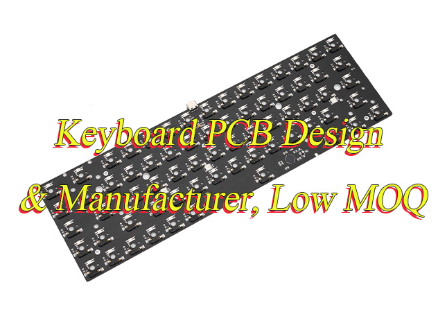
How to design a keyboard PCB? Let’s explore material selection, design software, design guide, technical parameter for keyboard PCB design.
Are you troubled with these problems?
- How to overcome the dual challenges of key signal crosstalk and electromagnetic interference under high-density layout?
- How to achieve cost-effective small-batch prototyping while maintaining flexible scalability for large-order rapid turnover?
- How to ensure full-cycle timeliness from design verification to mass production delivery, avoiding project delay risks?
As a keyboard PCB manufacturer, EBest Circuit (Best Technology) can provide you service and solutions:
- Electromagnetic Compatibility Optimization Plan: Adopt optimized differential signal routing + intelligent ground plane segmentation technology to achieve 30% improvement in signal integrity and reduce crosstalk to industry-leading levels.
- Flexible Capacity Management Platform: Modular production architecture supports 10-piece prototyping without price surcharge and enables 48-hour rapid response for 10,000-piece rush orders, boosting inventory turnover by 50%.
- Rapid Delivery Guarantee System: Full-process standardized management from DFM manufacturability verification to final product testing ensures 48-hour delivery for standard orders and compresses complex project cycles to 70% of industry average duration.
Welcome to contact us if you have any request for keyboard PCB design: sales@bestpcbs.com.
How to Choose Materials for Keyboard PCB Design?
A detailed guide to how to choose materials for keyboard PCB design:
Substrate Type Selection
- Prioritize FR4 epoxy fiberglass substrate for most consumer-grade keyboards, balancing cost and electrical stability. For high-strength scenarios, upgrade to 2.0mm thickness or use aluminum substrates to enhance heat dissipation and structural rigidity.
- Flexible keyboard designs require polyimide (PI) substrates, with validation of bend resistance cycles and lamination process compatibility.
Electrical Performance Parameters
- Dielectric constant (Dk) must remain stable within the recommended 4.2–4.8 range, with dissipation factor (Df) ≤0.015 to ensure signal integrity without delay or crosstalk. High-speed signal lines (e.g., USB interfaces) require strict 50Ω impedance matching, with Dk variation controlled within ±5%.
- For high-frequency RGB lighting or switches, use high-frequency specialized substrates (e.g., PTFE, ceramic-filled) with Df <0.005 to minimize signal loss.
Thermal Management Requirements
- Standard scenarios require high-Tg FR4 (Tg ≥130°C) to prevent solder joint thermal failure. High-heat scenarios (e.g., RGB-backlit keyboards) utilize aluminum substrates (thermal conductivity ≥1.0 W/m·K) or copper substrates for enhanced heat dissipation.
- Coefficient of thermal expansion (CTE) must match copper foil to prevent pad detachment under temperature changes, with recommended CTE ≤15ppm/°C.
Environmental Compliance & Regulations
- EU markets require compliance with RoHS 3.0 and REACH regulations, prohibiting hazardous substances like lead and halogens. Asian markets prioritize UL-certified eco-friendly substrates.
- Industrial/outdoor keyboards need salt spray test certification, using moisture- and corrosion-resistant enhanced FR4 (glass fiber content ≥30%).
Special Process Compatibility
- High-density designs (e.g., blind/buried vias, back-drilling) require substrates compatible with HDI processes. Ultra-thin keyboards use 1.0mm ultra-thin FR4 or flexible PI substrates to ensure manufacturing yield.
- Modular designs adopt recyclable bio-based epoxy resins to extend product lifecycle and reduce electronic waste.
Common Software for Keyboard PCB Design
- Altium Designer: A comprehensive professional-grade tool supporting end-to-end design from schematic to layout and routing, ideal for complex projects.
- KiCad: An open-source, free software offering schematic design, PCB layout, and 3D visualization, suitable for small-to-medium projects and individual developers.
- Autodesk Eagle: Geared toward small-to-medium designs, featuring a clean interface and free tier, commonly used for entry-level and rapid prototyping.
- Cadence OrCAD: A professional-grade solution enabling advanced simulation and collaboration features, designed for industrial-grade complex circuit design.
- PADS PCB Design: Focused on streamlining the design process, providing efficient layout and debugging tools for small-to-medium circuit board projects.
- EasyEDA: A cloud-based, free tool integrating shared libraries and collaboration capabilities, perfect for quick design and project sharing.
- Fritzing: Targeted at makers and hobbyists, offering simplified PCB design capabilities for educational and small-scale projects.
How to Design Your Own Keyboard PCB?
Below is a guide to keyboard PCB design:
1. Clarify Design Goals and Requirements
- Keyboard Type and Layout: Refine mechanical keyboard switch selection (e.g., Cherry MX, Gateron), optimize membrane keyboard tactile feel, and customize keycap compatibility for personalized keyboards. Layout specifications include full-size (104 keys), 60% (68 keys), split (e.g., Ergodox) key spacing and ergonomic tilt angles (e.g., 5°-12° keycap inclination), with support for hot-swappable socket types (e.g., 3pin/5pin MX-compatible).
- User Scenario Adaptation: Office scenarios prioritize low-noise switches (e.g., silent red switches) and anti-misoperation Fn key combinations. Gaming scenarios require 0.1ms response speed, programmable macro keys, and dynamic RGB lighting (e.g., wave mode, breathing light). Portable scenarios focus on lightweight design (e.g., acrylic case), Bluetooth/wired dual-mode connectivity, and battery life (e.g., 5000mAh lithium battery supporting 300 hours of standby).
- International Standards and Ergonomics: Adhere to ANSI/ISO dual-standard key mapping and support multilingual switching (e.g., Chinese/English, Japanese kana input). Ergonomic optimizations include keycap curvature (e.g., spherical keycaps), wrist rest silicone pads, and adjustable tilt brackets (e.g., three-stage foot supports).
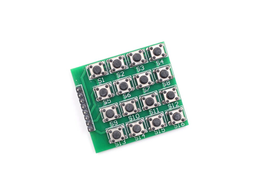
2. Plan Circuit Architecture and Matrix Design
- Matrix Design Balance: Utilize dynamic scanning algorithms to optimize row/column ratios (e.g., 8×16 matrix), eliminate “ghosting” via reverse-parallel diodes, and support NKRO (n-key rollover) mode.
- Main Controller Selection: Choose ARM Cortex-M4/M7 series (e.g., STM32F411) or dedicated keyboard MCUs (e.g., ATmega32U4), integrating USB HID protocol stacks, multi-key parallel recognition logic, and macro command storage (e.g., 128KB Flash supporting 500 macro instructions).
- Power Management Module: Implement 3.3V regulation via LDOs (e.g., TPS73733), integrate over-voltage protection (OVP), over-current protection (OCP), and ESD protection (e.g., TVS diode arrays), with low-power modes achieving standby current below 1μA (achieved via sleep mode + wake-up interrupts).
3. Layout and Signal Integrity Optimization
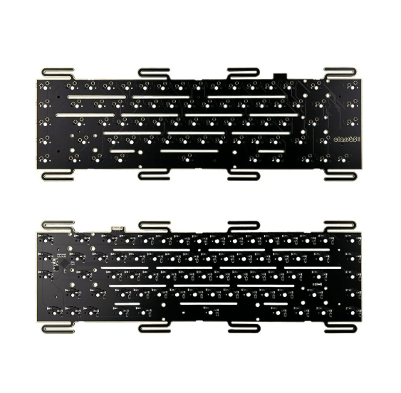
- PCB Layers and Stackup: Employ 4-layer board structure (signal layer – power layer – ground layer – signal layer), control USB differential line impedance at 90Ω±10%, minimize trace width/spacing to 4mil/4mil, and use blind/buried via processes to reduce signal crosstalk.
- Pad and Keycap Fixing: Hot-swappable pads compatible with MX switches (19.05mm pitch), keycap fixation supporting PCB mount (screw-fixed) or onboard snap-fit designs, with ENIG (electroless nickel gold) surface treatment for improved solderability.
- High-Speed Signal Processing: USB data lines use equal-length routing (±5mil error), differential pairs maintain 3x line width spacing, add common-mode chokes to suppress EMI, and place ESD protection devices near interface terminals (e.g., USBLC6-2SC6).
4. Interface and Extension Function Design
- USB Interface Specification: Type-C supports reversible insertion, CC pin configured with 5.1kΩ pull-up resistor for PD fast-charging recognition, DP/DM signal allocation complies with USB 2.0/3.0 electrical specifications, supporting data rates up to 480Mbps.
- Integrated Extension Functions: I2C interface connects OLED displays (128×32 resolution), SPI interface drives RGB light strips (WS2812B), programmable knobs read analog signals via ADC for volume/brightness adjustment, and reserved PMOD interfaces support sensor expansion (e.g., accelerometers).
- Debugging and Firmware Update: Integrated SWD interface (2.54mm pitch) supports ISP programming, test points (matrix nodes, power pins) facilitate multimeter/logic analyzer debugging, and firmware updates are achieved via DFU mode for wireless upgrades (e.g., Bluetooth OTA).
5. Maintainability and Compatibility Design
- Modular Structure: Main control board and sub-board separated via 24-pin FPC connectors, supporting hot-swappable upgrades (e.g., controller chip upgrades), positioning plates compatible with steel/acrylic/PC materials, and standardized assembly via M2 screw holes.
- Cross-Platform Compatibility: Firmware compatible with QMK/ZMK open-source frameworks, supports multilingual key mapping (e.g., layout switching via key combinations), cross-OS compatibility with Windows/macOS/Linux and Android/iOS devices, plug-and-play without driver installation.
- Expandability Design: Reserved expansion interfaces (e.g., GPIO pins) support future upgrades (e.g., adding touchpads), case design supports magnetic keycap replacement and custom sticker areas.
6. Verification and Testing Process
- Simulation Verification: Validate signal integrity via IBIS models, analyze power distribution network (PDN) impedance (target below 0.1Ω), optimize thermal design using thermal imaging simulation (e.g., Flotherm tools) to ensure operating temperatures below 65℃.
- Prototype Testing: Verify full-key no-ghosting via matrix scanning algorithms, test USB communication stability via 100,000 plug-in cycles, and measure power consumption for dynamic current monitoring (e.g., standby current below 100μA, operating current below 50mA).
- Compatibility Testing: Cover Windows 7/10/11, macOS 12+/Linux (Ubuntu/Debian), and Android 11+/iOS 15+ devices, validate HID protocol compatibility and multi-device switching response times (below 500ms).
7. Documentation and Design for Manufacturability (DFM)
- Production Documentation: Generate BOM lists (including component models, suppliers, inventory info), Gerber files with layer stackup, solder mask openings, drilling files, coordinate files for SMT machine assembly, and specify PCB parameters (e.g., 1oz/2oz copper thickness, HASL/ENIG surface finish, solder mask color like black matte).
- DFM Optimization: Tolerance for pad dimensions ±0.1mm, minimum trace width/spacing 4mil/4mil, via types use buried+blind via combinations to reduce interlayer crosstalk, panelization employs V-cut scoring + stamping holes for improved production efficiency.
- Version Control: Use Git for design change tracking, version numbers follow semantic versioning (e.g., v1.0.0), design documentation includes change logs, test reports, and multilingual user manuals.
Keyboard PCB Design Technical Parameter
| Technical Parameter | Typical Value / Range |
| PCB Thickness | 1.2mm, 1.6mm |
| Form Factor & Layout | ANSI, ISO, TKL, 60% etc. |
| Mounting Holes | Compatible with GH60 and other standards |
| Layer Count | 2-layer, 4-layer |
| Copper Thickness | 1 oz (35μm) |
| Min Trace/Space | 0.15mm (6 mil) |
| Power Trace Width | 0.4mm – 0.8mm |
| Switch Type | Mechanical, Hot-swappable, Magnetic |
| Matrix Scan Rate | 1kHz – 10kHz |
| Debounce Time | 5ms – 25ms |
| Main Controller Interface | USB Type-C |
| Connectivity | Wired, Tri-Mode (2.4G/Bluetooth/Wired) |
| Report Rate | 1kHz, 8kHz |
| RGB Lighting | Supports WS2812B etc. |
| Firmware Support | QMK, VIA, VIAL |
| ESD Protection | Integrated TVS Diodes |
| Surface Finish | ENIG, HASL, Immersion Gold |
| Solder Mask Color | Multiple options (Green, Black, White etc.) |
| Min Via Diameter | 0.3mm |
Keyboard PCB Layout & Routing Techniques
Efficient Key Matrix Layout
- Partition Optimization: Adopt “checkerboard” or “staggered” partition designs, grouping keys by functional modules (e.g., letter zone, number zone, function key zone, edit zone) to reduce cross-region routing length and signal crosstalk risk. For 60% layout keyboards, balance key spacing (typically 18-19mm) and routing density in compact spaces, avoiding signal cross-talk in high-frequency areas like WASD gaming zones. 65%/75% layouts can add dedicated arrow key or F-row partitions for enhanced usability.
- Row/Column Routing Strategy: Implement orthogonal layouts for row and column lines to avoid long parallel traces; critical row/column lines can be widened to 0.2-0.25mm to reduce signal delay and improve matrix scanning stability. For full-size (100%) keyboards, “serpentine” routing can minimize cross-layer vias and signal reflection risks.
Power and Ground Network Design
- Power Layer Segmentation: In 4-layer PCBs, design Layer 2 as a solid ground plane, and Layer 3 as segmented power domains (e.g., 5V, 3.3V, 1.8V) connected to top-layer power traces via vias, forming low-impedance return paths. Power trace widths should adapt to current requirements: USB input traces 0.4-0.8mm wide, LED backlight power traces ≥1mm wide, and MCU power traces 0.3-0.5mm wide. A π-type filter circuit (10μF electrolyytic capacitor + 0.1μF ceramic capacitor + 10Ω resistor) can be added near USB ports to suppress power noise.
- Grounding Strategy: Deploy dense grounding vias (spacing ≤5mm) near MCUs and LED backlight modules to form “ground islands” reducing EMI. ESD protection devices (e.g., TVS diodes) must be placed close to interfaces, with ground terminals directly connected to the ground plane to ensure the shortest electrostatic discharge path. For multi-layer boards, “ground via arrays” can enhance inter-layer connectivity and reduce ground impedance.
High-Speed Signal and Backlight Routing
- RGB Backlight Routing: WS2812B LED data lines require 50Ω impedance matching, using “serpentine” length-matching traces for signal synchronization. Avoid parallel routing with power lines (spacing ≥0.3mm) to minimize crosstalk. Power lines should be widened to ≥1mm and equipped with 100nF decoupling capacitors near LEDs to suppress power noise. For long LED chains, “segmented power supply” designs (adding independent power nodes every 10-15 LEDs) can reduce voltage drop.
- USB Differential Pair Optimization: USB Type-C differential pairs (D+/D-) must maintain equal length (error ≤5mil), equal spacing (10-15mil), and trace length ≤200mm without cross-layer vias. Top-layer differential pairs can be wrapped with ground shielding traces (spacing 0.1-0.2mm), while inner-layer pairs should neighbor ground planes to reduce EMI radiation. For USB 3.0/3.1, “impedance-controlled” routing with ±10% tolerance and common-mode chokes are required to suppress EMI.
Signal Integrity Enhancement
- Debouncing and Matrix Scanning: Add RC filter circuits (1kΩ resistor + 10nF capacitor) at row/column line ends, combined with 5-25ms software debouncing time to reduce false key triggers. For high-frequency scanning (1kHz-10kHz), shorten row/column line lengths (≤50mm) to avoid signal reflections. Mechanical keyboards can adopt “hardware debouncing” chips (e.g., MAX7360) for faster response.
- Impedance Control: Critical signal lines (e.g., clock, data) should be designed with impedance calculation tools (e.g., Saturn PCB) within ±10% tolerance. Sensitive signals (e.g., backlight data) should avoid proximity to high-frequency noise sources (e.g., switching power supplies, crystals) and use “shielding layers” for enhanced noise immunity.
Manufacturability and Testability
- Minimum Trace Width/Spacing: Strictly adhere to 0.15mm (6mil) minimum trace width/spacing specifications to avoid manufacturing defects. Via sizes should be ≥0.3mm (minimum hole size) with “thermal relief” designs for better adhesion. For high-density routing, “blind/buried vias” can reduce inter-layer connection lengths.
- Test Point Layout: Reserve test points (diameter ≥1mm) at MCU pins, power nodes, and critical signal paths for ICT testing and debugging. Surface finishes (e.g., ENIG, HASL) should be selected based on soldering requirements to ensure solderability. For automated testing, “test point arrays” can improve testing efficiency.
Thermal Management and EMC Design
- Thermal Design: Add thermal via arrays (≥10 vias/cm²) under high-power components (e.g., LEDs, power management chips), with top-layer copper pours connected to the ground plane. Avoid stacking heat sources and maintain ventilation gaps (≥2mm). For high-heat chips, use “heat sinks” or “thermal pads” to enhance heat dissipation.
- EMC Protection: Add a GND ring at the keyboard edge to reduce external interference. High-frequency clock signals (e.g., MCU crystals) should be wrapped with ground shielding (spacing 0.1-0.2mm) to avoid radiation exceedances. Common-mode chokes near connectors can suppress 2.4G/Bluetooth antenna interference. For wireless keyboards, “EMI filters” enhance noise immunity and ensure CE/FCC compliance.
Open Source Keyboard PCB Design Projects
- Caldera Keyboard: Based on Ergogen tool for generating configuration files, supports PCB design, firmware programming, and 3D printed cases. Ideal for personalized input devices, tech enthusiast learning, educational tools, and prototyping. Features include high customization, open-source friendliness, compatibility with KiCad manufacturing, and video tutorials to reduce learning curves.
- Plain60-C: 60% minimalist layout open-source mechanical keyboard PCB designed in KiCad, compatible with QMK firmware and VIA configurator. Supports USB-C interface, ESD protection, JST connectors, and fits standard 60% cases or HHKB/WKL Tofu layouts. Key traits: compact layout, no LED decorations, ISP header for firmware flashing, optimized component placement for improved soldering experience.
- hotswap_pcb_generator: Parametric design tool based on OpenSCAD for auto-generating MX/Choc switch keyboard PCBs, bottom plates, and cases. Supports TRRS socket integration, non-standard grid spacing, and adapts to KLE layout files. Highlights: one-click 3D model generation, rapid design iteration, community extension support, suitable for prototyping and customization.
- AI03 Keyboard PCB Guide: Open-source GitHub project containing KiCAD circuit design files, firmware code, and documentation. Clear directory structure: src for design files, assets for example images, LICENSE specifying open-source terms. Offers installation steps, contribution guidelines, ideal for developers to deep-dive into keyboard circuit design logic.
- Pocket Keyboard: Compact open-source keyboard project designed in EasyEDA, running TMK firmware. Uses Atmega32u4 microcontroller, supports Micro USB interface, and 16MHz crystal. Advantages: portable and cost-effective, supports custom key mapping, suitable for mobile work and developer testing scenarios.
- EC60: 60% electrostatic capacitive PCB keyboard supporting Topre/NIZ switches, utilizing STM32F401 microcontroller. Compatible with QMK firmware, integrates USB-C and JST connectors, includes ESD protection and fuse design. Strengths: high durability, compatible with various PCB manufacturers, supports VIA/VIAL configuration, tailored for professional office and gaming use.
- chocV Project: 40% Choc keyboard with dual-PCB design for low-profile form factor, based on Horizon construction method. Supports Miryoku layout, compatible with QMK/ZMK firmware. Features: protected component design, flexible layout adjustments, updated Gerber files for optimized manufacturing, ideal for custom keyboard enthusiasts.
- Djinn Keyboard: Split 64-key keyboard with dual 4×7 matrix plus 5-way tactile switch. Sub-board Ghoul enables hot-swap MCU, RGB OLED, and per-key RGB lighting. Attributes: QMK firmware compatibility, supports SparkFun MicroMod features, suited for users requiring advanced customization capabilities.
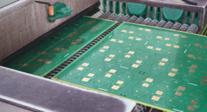
How to Make A Keyboard PCB Board?
1. Material Cutting and Panelization
- Material Selection: Use high-Tg FR4 substrate (e.g., TG150-180) to prevent deformation during high-temperature soldering. Copper foil thickness is typically 18μm or 35μm to meet current-carrying and etching precision requirements.
- Panelization Optimization: Combine UNIT (single-key unit) and SET (multi-unit panel) layouts, reserving ≥5mm process edges for clamping and positioning. Add quincunx-shaped positioning holes (diameter 1.2mm±0.1mm) to ensure lamination alignment accuracy ≤±0.05mm. Edge etching markers facilitate AOI automatic inspection.
2. Drilling and Hole Metallization
- Precision Drilling: Utilize CNC drilling machines to create through-holes (diameter 0.3-0.8mm), blind holes (depth ≤1.2mm), and buried holes. Control hole wall roughness Ra≤3.2μm to avoid plating defects.
- Hole Metallization Process: Form a 0.3-0.5μm copper layer via chemical deposition, then electroplate to 20-25μm thickness using pulse plating for uniformity. Hole copper tensile strength must ≥15N/mm² to ensure conductivity reliability.
3. Imaging and Etching
- Dry Film Application and Exposure: Apply 10-20μm dry film via automatic laminators. Achieve ±10μm line width/spacing accuracy using LDI (Laser Direct Imaging) with exposure energy 18-22mJ/cm². Developed line width tolerance is ±0.05mm.
- Etching Control: Use vertical spray etching machines with etchant temperature 45-50℃ and pressure 2.0-2.5bar. Etching rate is 1.0-1.2μm/min, monitored in real-time by online systems to prevent over-etching or residual copper.
4. Lamination and Stack-up Structure
- Multilaminate Lamination: Enhance bonding via black oxide treatment on inner cores. Stack prepreg (e.g., 1080-type PP) symmetrically and cure under vacuum at 180-200℃, 25-30MPa for 2 hours. Interlayer alignment accuracy ≤50μm.
- Impedance Control: Design microstrip/stripline structures based on signal characteristics. Adjust dielectric constant (εr=4.2-4.8) and line width/spacing to achieve USB differential line impedance of 90±7Ω, validated by TDR testing.
5. Outer Layer Plating and Solder Mask
- Outer Layer Plating: Electroplate copper to 20-25μm thickness, with tin layer 1.0-1.5μm as etch resist. Strip tin post-etching to reveal final circuitry.
- Solder Mask and Silkscreen: Screen-print solder mask (e.g., matte black, green) at 20-30μm thickness, cured via UV exposure (500-800mJ/cm²). Silkscreen uses white epoxy ink with ±0.1mm printing accuracy for clear component identification.
6. Surface Finish Options
- ENIG (Electroless Nickel Immersion Gold): Nickel layer 3-5μm, gold layer 0.05-0.1μm for enhanced solderability and oxidation resistance, suitable for high-frequency applications.
- HASL (Hot Air Solder Leveling): Tin-lead alloy (Sn63/Pb37) coating 3-8μm thick, cost-effective but with lower surface flatness, ideal for consumer keyboards.
- OSP/Immersion Silver/Immersion Tin: OSP thickness 0.2-0.5μm for lead-free compliance; immersion silver/tin 0.1-0.3μm for high-frequency signal integrity.
7. Profiling and Cutting
- CNC Profiling: Diamond-coated tools cut contours at 15-20m/min speed, 0.1-0.2mm/rev feed. Edge chamfering (R0.2-0.5mm) prevents burrs.
- V-Scoring: Pre-cut V-grooves (depth 1/3 board thickness) between panels for manual/mechanical separation, minimizing stress damage.
8. Electrical Testing and Functional Verification
- Flying Probe Testing: Four-wire testing detects opens, shorts, and impedance anomalies with ≥50μm test point spacing and ±2Ω accuracy. Covers key matrix, LED backlight, USB interface connections.
- Full Functional Testing: AOI detects surface defects (scratches, exposed copper). HID-TEST simulates key presses to validate matrix scanning logic and anti-ghosting. USB interfaces undergo signal integrity tests (e.g., eye diagram analysis).
9. Packaging and Shipping
- Quality Inspection: 50x magnification confirms no oxidation/scratches. Dimensional checks use CMM with ±0.1mm tolerance. Hole diameter and board thickness verified via calipers/thickness gauges.
- Vacuum Packaging and Traceability: Anti-static vacuum bags with desiccants and humidity cards. Include BOM, Gerber files, and QC reports. QR codes enable batch traceability.
Why Choose EBest Circuit (Best Technology) as Keyboard PCB Manufacturer?
Reasons why choose us as keyboard PCB manufacturer:
- Global Compliance Certifications for Export Readiness: Products meet UL safety standards, RoHS environmental compliance, and REACH regulations, ensuring smooth market entry in major regions like EU, US, Japan, and Korea. Full material certifications and test reports are provided.
- 19 Years of Industry Expertise: Established in 2006, we’ve served 500+ global keyboard brands and developed 2000+ customized PCB solutions. Our extensive case library accelerates development cycles by 30%, backed by proven expertise.
- Rapid Prototyping & Flexible Small-Batch Production: Support single-piece sample production with 72-hour express prototyping. Low MOQ starts at 10 pieces for volume production, perfectly accommodating prototype validation and small-batch trials without delays.
- Transparent Pricing with Zero Hidden Costs: Tiered pricing system ensures full cost transparency. No additional fees, material and process costs are clearly itemized. Unit prices are 15-20% lower than industry averages, delivering unbeatable value.
- Free DFM Analysis for Manufacturability Forecasting: Professional DFM reports identify potential production risks during the design phase. Through 3D simulation and process verification, 95%+ manufacturability issues are resolved upfront, minimizing rework costs.
- End-to-End One-Stop Solutions from Design to Assembly: Full-service coverage includes circuit design optimization, SMT placement, through-hole assembly, and functional testing. Clients provide concepts; we handle seamless execution from concept to finished product, reducing communication overhead by 30%.
- Strict Quality Control System: ISO9001/TS16949 dual certification ensures rigorous quality management. Triple inspection protocols, AOI optical inspection, X-ray analysis, and flying probe testing, ensure defect rates below 0.03%, exceeding industry standards.
- Advanced Flexible Production Lines for Complex Needs: Equipped with high-precision LDI exposure machines and AOI systems, supporting advanced processes like HDI blind vias and rigid-flex boards. Minimum trace/space of 3mil meets precision requirements for high-end mechanical keyboards.
- Dedicated 24/7 Engineering Support Team: Over 10 senior engineers provide end-to-end project tracking. 48-hour online technical support ensures 2-hour response and 8-hour resolution for issues, guaranteeing smooth project execution.
Welcome to contact us if you have any request for keyboard PCB board: sales@bestpcbs.com.
You may also like


Tags: keyboard pcb, Keyboard PCB Design