

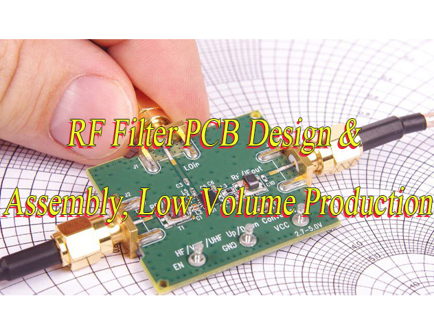
Why choose RF Filter PCB? Let’s discover components, applications, technical parameter, layout and design guide, assembly process for RF filter PCB.
Are you worried about these problems?
- How to ensure stable RF filtering performance without signal attenuation during high-frequency signal transmission in multi-layer PCBs?
- How to guarantee pure high-frequency signal integrity at 5G/millimeter-wave bands amid severe cross-layer signal interference?
- How to quickly resolve performance inconsistencies caused by high-frequency soldering defects during mass production?
As a RF filter PCB assembly manufacturer, EBest Circuit (Best Technology) can provide you service and solution:
- Precise optimization of high-frequency signal paths: 3D electromagnetic simulation for trace layout design reduces transmission loss by 15%, ensuring stable RF filtering performance.
- Multi-layer board-level signal isolation process: Layered shielding and microstrip line impedance matching technology effectively suppress cross-layer interference, improving high-frequency signal purity by 20%.
- Rapid response high-frequency soldering task force: High-precision laser soldering equipment and AI vision inspection system enable defect analysis and process optimization within 24 hours, stabilizing batch yield above 98% and accelerating product delivery cycles.
Welcome to contact us if you have any request for RF filter PCB design & assembly: sale@bestpcbs.com.
What Is RF Filter PCB?
A RF filter PCB is a printed circuit board specifically designed for radio frequency (RF) filters. Through precise design of circuit layout and high-frequency materials, it enables efficient filtering or retention of specific frequency band signals in wireless communication, radar, or satellite systems. This effectively suppresses interference, improves signal quality, and serves as the core hardware carrier ensuring stable RF front-end performance.
Components of RF Filter PCBs
Passive Components
- Capacitors/Inductors/Resistors: Form the foundation of RC/LC filters (e.g., elliptic filters, SAW filters, BAW filters) for frequency selection and suppression. For instance, 0.01μF ceramic capacitors outperform 0.1μF in high-frequency filtering (>50MHz).
- Ferrite Beads: Suppress high-frequency noise by forming T-type/π-type filter networks with capacitors/inductors, adapting to source/load impedance characteristics.
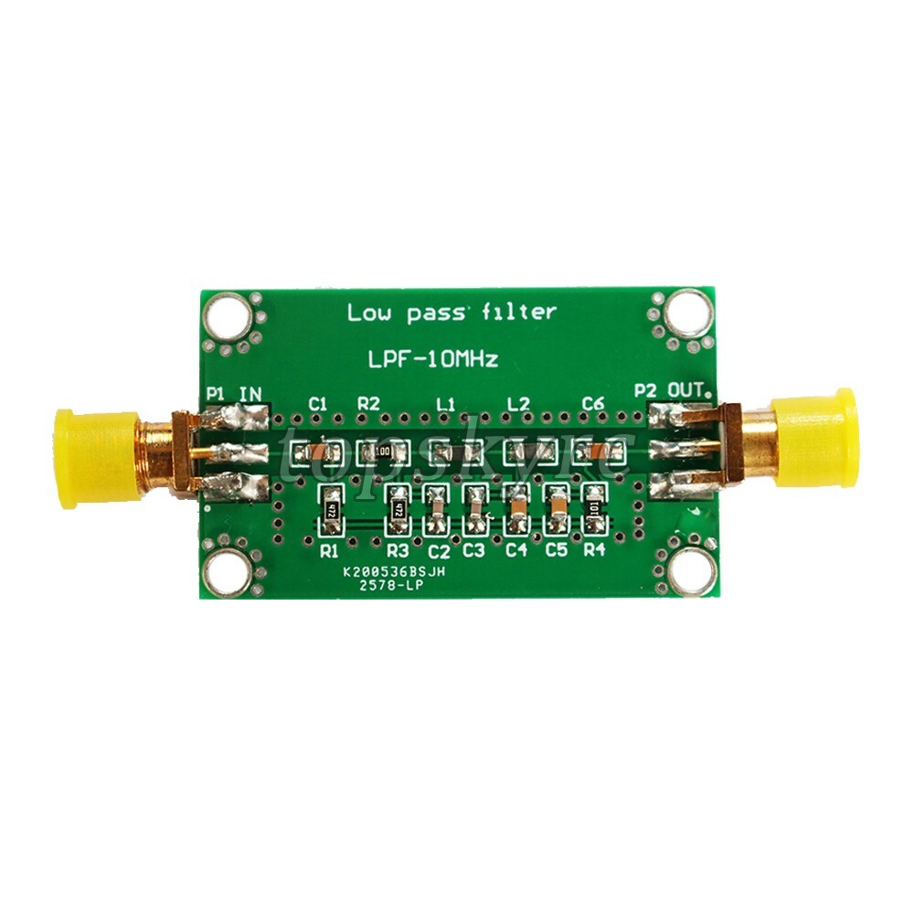
Transmission Lines & Microstrip Lines
- Microstrip/Stripline: Control 50Ω/75Ω characteristic impedance to connect filters, amplifiers, etc. Avoid sharp bends; use 135° angles or Duvall-James formula for impedance compensation.
- Coplanar Waveguide (CPW): Isolate signal lines via ground via fences to minimize crosstalk, suitable for high-frequency signal transmission.
Grounding & Shielding Structures
- Ground Plane: Solid ground layer (e.g., PCB Layer 2) provides low-impedance reference ground, reducing ground loop noise.
- Ground Vias/Rings: Ground via spacing ≤1mm, ground ring width 1-2mm to form isolation bands and suppress EMI (e.g., ground rings around filters to isolate external noise).
- Shielding Measures: Isolate digital/analog ground to avoid shared impedance coupling; antenna clearance zone radius ≥λ/4 (e.g., 30mm for 2.4GHz), with ground rings at edges.
Filter Chips
- SAW/BAW Filters: Use CSP or flip-chip packaging (sizes as small as 1.4mm×1.1mm). Match CTE to avoid stress issues between ceramic substrates and PCBs.
- LC Filters: Composed of inductors/capacitors, offer steep transition bands for high-frequency bands (e.g., 5G NR).
Power Management Components
- Decoupling Capacitors: Parallel 100pF (high-frequency) and 10μF tantalum (low-frequency) capacitors to suppress >1MHz switching noise, placed ≤2mm from power pins.
- Inductors: For power filtering (e.g., 1μH inductor + capacitor LC network) to reduce power ripple.
Antenna-Related Components
- PCB Antennas: Such as inverted-F/monopole antennas, placed on isolated PCB edges (e.g., center of long edges) with clearance zones (no copper/vias), radiating toward unobstructed areas.
- External Antenna Connectors: Such as SMA/IPEX connectors, positioned near PCB edges with axis parallel to edges (≤5° deviation), ground shells connected via 3-4 ground vias to RF ground.
Advantages of RF Filter PCB
- Superior High-Frequency Performance: Designed specifically for high-frequency signals, RF Filter PCBs utilize materials with optimized dielectric constants (e.g., FR-4, Rogers) to minimize signal loss and delay, ensuring stability in high-frequency bands such as 5G and Wi-Fi.
- Integration and Miniaturization: Through advanced layout techniques like microstrip lines and striplines, filters can be directly embedded into the main circuit board, saving space and enabling compact device designs (e.g., smartphones, IoT terminals).
- Cost Efficiency: Compared to discrete components or cavity filters, PCB-based designs reduce assembly steps, lower material and production costs, and are ideal for mass production.
- Design Flexibility: Supports customizable topologies (e.g., bandpass, low-pass filters) and allows rapid parameter adjustments via simulation tools like ADS, adapting to diverse frequency bands and impedance requirements.
- Reliability and Consistency: Standardized PCB manufacturing processes ensure stable electrical characteristics, minimize manual assembly errors, enhance anti-interference capabilities, and extend product lifespan.
- Easy Testing and Debugging: Test points can be integrated directly onto the board surface, enabling quick calibration with Vector Network Analyzers (VNAs) and streamlining production quality control.

Applications of RF Filter PCB
- Wireless Communication Devices
- Satellite Communication Systems
- Radar & Military Electronics
- Medical Device
- Testing & Measurement Instruments
- IoT Terminals
- Automotive Electronics
- Consumer Electronics
- Industrial Control
- Aerospace
RF Filter PCB Design Technical Parameter
| Specific Parameter | Typical Value / Requirement |
| Dielectric Constant (εr) | 2.2-3.55 (e.g., Rogers RO4003 series) |
| Loss Tangent (Tan δ) | ≤0.0027 (e.g., RO4003C) |
| Substrate Thickness | 0.76mm (60 mils) |
| Characteristic Impedance | 50Ω |
| Line Width / Spacing Tolerance | ±20/25μm (at conductor height ~45μm) |
| Transmission Line Type | Microstrip, Coplanar Waveguide (CPW) |
| Center Frequency | Application-specific (e.g., 6GHz) |
| Bandwidth | Application-specific (e.g., 20% bandwidth) |
| Insertion Loss | <1.5dB |
| Return Loss | >14dB |
| Out-of-Band Rejection | e.g., 46dB @ 2.388GHz |
| Copper Foil Thickness | 0.5oz-2oz (17.5-70μm) |
| Surface Finish | ENIG (Electroless Nickel Immersion Gold), Immersion Silver |
| Via Type | Shielding Vias, Ground Vias |
| RF-Digital Spacing | >1cm (recommended ≥2cm) |
| Power Decoupling | Decoupling capacitor per power pin |
| Connector Type | SMA, SMB |
RF Filter PCB Layout & Routing Technique
1. Partitioning and Layout Planning
- Thermal-Electric Co-Design Partitioning: When laying out high-power RF devices (e.g., Power Amplifiers), integrate thermal simulation to reserve heat dissipation paths, avoiding thermal concentration that affects filter stability. Keep low-noise regions (e.g., LNA front-end) at least 3mm away from heat sources to minimize temperature drift errors.
- Modular Isolation Strategy: For multi-band filter groups, adopt an “island-style” layout where each filter module is independently partitioned and surrounded by ground via arrays to prevent cross-module interference. Add isolation strips near critical interfaces (e.g., SMA connectors) to suppress external interference intrusion.
- 3D Signal Flow Optimization: In multi-layer PCBs, utilize inner-layer routing to vertically separate input/output signals (e.g., top-layer input, bottom-layer output) with ground layers providing isolation to reduce planar coupling. Prioritize complete ground planes beneath sensitive signal layers to avoid signal cross-layer traversal through split zones.
2. Stackup and Grounding Design
- Stackup Parameter Precision Design: Based on target impedance (e.g., 50Ω) and substrate characteristics (e.g., FR4 dielectric constant 4.2–4.8), precisely calculate microstrip line width, spacing, and dielectric thickness. For high-frequency bands (e.g., millimeter-wave), use low-loss substrates (e.g., Rogers RO4350B) and optimize stackup order to minimize dielectric losses.
- Grounding Topology Enhancement: Adopt a hybrid “mesh ground + solid ground” structure—mesh ground on outer layers reduces eddy current losses, while solid ground on inner layers provides low-impedance paths. Filter ground pins must connect to the ground plane via ≥3 vias to reduce grounding inductance.
- Via Array Optimization: Surround filters with ground via arrays (Via Fence) spaced at λ/20 (λ = operating wavelength) to form electromagnetic shielding walls. Vias must be securely soldered to the ground plane to prevent solder joint failure.
3. Transmission Line and Impedance Control
- Transmission Line Type Selection: Microstrip lines suit frequencies ≤6GHz; coplanar waveguides (CPW) offer better radiation suppression at ≤3GHz. Differential RF signals require symmetric coplanar waveguides (GCPW) to ensure differential pair impedance consistency.
- Impedance Matching Refinement: Optimize trace length, width, and spacing via tools like ADS/HFSS for precise impedance matching. Reserve tuning segments at critical nodes (e.g., filter I/O) for fine-tuning with series resistors or parallel capacitors.
- Corner Treatment and Serpentine Routing: Use 135° miters or curved corners to minimize impedance discontinuities. For length matching, employ serpentine routing with spacing ≥3× line width to avoid crosstalk.
4. Filter-Specific Layout Constraints
- Multi-Filter Co-Layout: Arrange multi-band filter groups by frequency descending order (e.g., 5GHz → 2.4GHz), placing high-frequency filters near antennas and low-frequency filters near baseband. Maintain ≥2mm spacing between adjacent filters with ground isolation strips.
- Filter-Matching Network Synergy: Directly connect filter I/O ports to matching networks (e.g., π-networks) without intermediate components. Position matching network components (capacitors/inductors) close to filter pins to minimize parasitic effects.
- Keepout Zone Management: Prohibit signal/power traces beneath filters; only ground copper is allowed. Connect bottom-layer ground copper to top-layer ground via multiple vias to form a “sandwich” shielding structure.
5. Power and Decoupling Design
- Multi-Stage Decoupling Strategy: Combine bulk electrolytic capacitors (low-frequency noise), film capacitors (mid-frequency), and ceramic capacitors (high-frequency) near power pins. Ground capacitor terminals directly to the ground plane via vias.
- Power Trace Isolation: Physically isolate RF power traces from digital/analog power traces to avoid cross-coupling. Size power traces based on current (e.g., 10mil/1A) and use shielded routing (e.g., grounded coplanar lines) to reduce radiation.
6. Shielding and Interference Mitigation
- Shielding Can Optimization: Use conductive materials (copper/aluminum) for grounded shielding cans. Seams adopt “finger-cross” structures or conductive adhesives for sealing. Matte-finish inner walls reduce internal reflections. Connect shields to PCB ground via spring contacts or solder pads for low-impedance grounding.
- EMI/EMC Enhancement Measures: Optimize port matching with series resistors (e.g., 50Ω) or parallel capacitors (e.g., 10pF) at filter I/O ports. Add EMI filters (e.g., π-filters) at critical interfaces (e.g., antenna ports) to suppress common-mode noise. Deploy ground via arrays along PCB edges to create a “Faraday cage” effect.
How to Design A RF Filter PCB?
Below is a RF filter PCB design guide:
1. Define Design Specifications & Topology Selection
- Refine Frequency Domain Metrics: Beyond center frequency and bandwidth, specify group delay fluctuation range (e.g., ≤2 ns@passband), form factor (e.g., BW3dB/BW20dB≤1.5), and phase linearity requirements to prevent time-domain signal distortion.
- Topology Adaptation Strategy: For low-frequency bands (<3 GHz), prioritize lumped LC structures; for high-frequency bands (>5 GHz), adopt microstrip interdigital/hairpin filters; for ultra-high frequencies (>10 GHz), recommend substrate integrated waveguide (SIW) or ceramic dielectric resonator solutions. Validate nonlinear effects via ADS harmonic balance simulation.
2. High-Frequency Substrate Selection & Stackup Design
- Substrate Performance Comparison: Rogers RO4350B (εᵣ=3.48, tanδ=0.0037) suits moderate loss scenarios, while Taconic RF-35 (εᵣ=3.5, tanδ=0.0021) offers lower loss at high frequencies. Balance cost and performance during selection.
- Stackup Optimization: 6-layer structures enable mid-layer stripline (layers 3-4) for signal-ground plane interleaving, reducing crosstalk. Bottom-layer ground planes require thermal pad designs to enhance heat dissipation.
3. Transmission Line Impedance Precision Control
- Microstrip Design Standards: For 50 Ω impedance, maintain line width/dielectric thickness ratio (W/H) within 1.8-2.2. At 17 μm copper thickness, FR-4 substrate (εᵣ=4.2) typically requires 2.5 mm line width.
- CPW Advantages: Coplanar waveguides achieve low dispersion via dual ground planes, ideal for broadband filters. Maintain signal-to-ground spacing (S) ≥2W to stabilize impedance.
4. Component Selection & Layout Optimization
- Capacitor Selection Criteria: NP0 capacitors must satisfy SRF>2f₀; C0G capacitors excel in high-temperature stability. For high-frequency bulk capacitance, use low-ESR tantalum capacitors or parallel MLCCs.
- Inductor Layout Rules: Wire-wound inductors should be perpendicularly staggered to avoid parallel magnetic coupling. Chip inductors require etched isolation trenches beneath pads to prevent parasitic capacitance with ground planes.
5. EMI Shielding & Decoupling Design
- Shielding Enclosure Design: Metal shields must connect to PCB ground via spring contacts (contact resistance <10 mΩ). Cavity height should exceed 2× filter thickness to avoid electromagnetic resonance.
- Decoupling Configuration: Implement π-type filtering (100 pF+10 nF+1 μF) at power pins, paired with ferrite beads for high-frequency noise suppression. Decoupling capacitors must be within 3 mm of power pins, with trace lengths <λ/20.
6. Simulation & Prototype Validation
- Simulation Workflow: Pre-simulation validates S-parameters, group delay, and power handling. Post-simulation incorporates PCB process parameters (e.g., etching factor, layer alignment tolerance) for tolerance analysis.
- Test Standards: Passband insertion loss <1.5 dB@center frequency; stopband rejection >40 dB@2f₀; group delay fluctuation <0.5 ns; phase distortion must meet eye diagram requirements.
7. DFM & Reliability Considerations
- Pad Design Standards: 0402 components adopt “dog-bone” pads (narrow center, wide ends) to mitigate tombstoning. BGA packages require solder thieving pads for enhanced reliability.
- Reliability Testing: Conduct thermal shock (-40℃~125℃, 500 cycles), vibration (10G, 2hrs), and salt spray (48hrs) tests to ensure stability in harsh environments.
8. Documentation & Production Handoff
- Production File Standards: Gerber files must include impedance control layers, copper thickness annotations, and keep-out zones. Provide 3D models (e.g., STEP format) for mechanical assembly verification.
- Production Coordination: Confirm substrate model, thickness tolerance, and surface finish with PCB manufacturers. Supply impedance test reports and cross-section validation to ensure manufacturing consistency.

How to Assemble A RF Filter PCB?
A detailed guide to RF Filter PCB Assembly Process:
1. Design Preparation and Material Selection
- Circuit Design & Simulation: Utilize professional tools (e.g., ADS, AWR) for circuit design and simulation to ensure performance metrics (bandwidth, insertion loss, return loss) meet requirements. Conduct multi-round iterative optimization and validate layout impact through EM simulation (e.g., HFSS).
- PCB Material Selection: Prioritize low-loss RF substrates (e.g., Rogers RO4003C, RO4350B, PTFE) with stable dielectric constant (Dk=3.38–3.48) and low loss tangent (Df≤0.0037@10GHz). Avoid FR4 for high-frequency applications. For mmWave (>30GHz), use ultra-low-loss materials (e.g., RO3003 series).
- Stack-up & Impedance Control: Strictly control 50Ω impedance design. Calculate trace width, dielectric thickness, and copper thickness using tools like SI9000, with tolerance ≤±5%. Optimize ground plane and signal isolation structures.
2. PCB Manufacturing and Pre-processing
- PCB Fabrication: Partner with RF-capable manufacturers, providing impedance control documentation (target impedance, trace width, reference layers) to ensure consistent etching accuracy, dielectric thickness, and copper thickness.
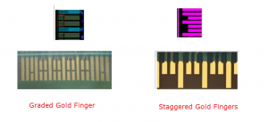
- Surface Finish: Select RF-compatible finishes (e.g., ENIG or immersion gold) to prevent oxidation and ensure solder reliability. Immersion gold thickness should be 0.05–0.1μm; thicker layers increase high-frequency loss.
- Cleaning & Baking: Clean and bake PCBs (125°C/2 hours) before assembly to remove moisture and prevent solder voids. Store in environments with humidity <30%RH.
3. Component Preparation and Mounting
- Component Procurement & Inspection: Source high-frequency components (RF inductors, capacitors, connectors), verify specifications, and measure critical parameters (Q-factor, self-resonant frequency). For critical components (e.g., filter chips), perform X-ray inspection of internal structures.
- Solder Paste Printing: Use laser-cut stainless steel stencils (0.1–0.15mm thickness) with SAC305 lead-free solder paste (3% silver content). Post-printing, perform 3D SPI inspection for volume/height deviations.
- Pick-and-Place Assembly: Employ high-precision pick-and-place machines (±0.05mm accuracy). Prioritize small components (0402/0201) followed by larger components/connectors. For BGA/QFN packages, use optical alignment systems to ensure pad-to-pin matching.
4. Soldering Process Control
- Reflow Soldering: Use nitrogen-purged reflow ovens (oxygen <100ppm) with Ramp-Soak-Spike profiles. Set peak temperature to 235–245°C with 40–60 seconds above 220°C to minimize thermal damage to RF components.
- Hand Soldering Supplement: For through-hole components, use temperature-controlled soldering irons (300–350°C) for quick soldering. Avoid acidic flux; clean residues with isopropanol.
- Shield Installation: After soldering, install Cu-Ni alloy shields with ground via spacing <λ/10. Fill gaps with conductive foam to enhance sealing.
5. Inspection and Testing
- Visual & X-ray Inspection: Conduct AOI for component misalignment/polarity errors. Verify BGA solder joint voids <25% via X-ray.
- Electrical Testing: Use VNA to measure S-parameters (S11, S21) and compare with simulation results. Perform SOLT calibration covering the operating frequency range (e.g., 1–20GHz).
- Functional Verification: Test out-of-band rejection and insertion loss by connecting to RF systems (signal generator + spectrum analyzer). For multi-channel filters, verify channel-to-channel isolation >30dB.
6. Environmental Reliability and Long-Term Validation
- Environmental Stress Screening: Subject assembled filters to temperature cycling (-40°C to +85°C, 1000 cycles, 30-minute dwell at extremes). Ensure impedance variation ≤10% and insertion loss change ≤0.2dB/10cm.
- Vibration & Shock Testing: Follow MIL-STD-810H standards for random vibration (5–500Hz, 5Grms) and mechanical shock (half-sine, 50G/11ms) to confirm no component detachment or solder joint cracking.
- Long-Term Aging Test: Perform 96-hour continuous operation at 85°C/85%RH. Monitor parameter drift (insertion loss change <0.1dB) to validate long-term reliability of components/solder joints.
- Protective Coating: Apply acrylic-based conformal coating with stable dielectric constant, shielding test ports/connectors to resist humidity, dust, and chemical corrosion.
7. Documentation and Continuous Optimization
- Data Logging and Traceability: Record PCB batch numbers, solder paste batches, and reflow profiles. Implement MES for tracking critical process parameters.
- Failure Analysis: For non-conforming units, perform cross-section analysis and SEM/EDS inspection to identify failure modes (e.g., excessive IMC layer, substrate delamination). Feed results back to design for iterative optimization.
- Process Specification Updates: Periodically review and update process documents to incorporate best practices from new materials (e.g., LTCC) and processes (e.g., laser drilling).
Why Choose EBest Circuit (Best Technology) as RF Filter PCB Assembly Manufacturer?
Reasons why choose us as RF filter PCB assembly manufacturer:
- One-Stop Full-Process Service: Covering design, prototyping, production, and assembly, clients avoid multi-supplier coordination, reducing communication costs and time, accelerating product launch cycles by over 40%.
- 19 Years of PCBA Service Expertise: Specializing in RF filter PCB assembly for 19 years, serving over 500 clients, mastering high-frequency signal transmission, material matching, impedance control, and core processes to ensure stable performance.
- Strict Quality Control System: Adopting ISO 9001-certified full-process quality monitoring, executing 12 rigorous testing procedures from raw material inspection to final testing, with a defect rate below 0.03%, significantly lower than industry averages.
- High-Frequency Specialized Assembly Technology: Proficient in RF-specific techniques such as microstrip precision soldering and via filling optimization, paired with high-precision placement machines (±0.02mm accuracy), ensuring lossless 5G high-frequency signal transmission and meeting strict requirements for low insertion loss and high isolation.
- Rapid Prototyping & Production Capability: Completing rapid prototyping within 72 hours and halving production cycles compared to conventional manufacturers, supporting flexible small-batch and multi-variety production for seamless transition from prototype to mass production.
- Customized Solutions: Providing tailored assembly solutions for various frequency bands (e.g., Sub-6GHz, millimeter wave) and package sizes (0201 components to large modules), combined with simulation software for thermal management and EMC optimization to enhance product competitiveness.
- Advanced Equipment & Processes: Equipped with fully automatic solder paste printers, X-ray inspectors, AOI optical detectors, and adopting lead-free soldering processes and nitrogen-protected environments to ensure soldering reliability and environmental compliance, meeting international standards like RoHS.
- Professional Team Support: A 20-member senior engineer team offering 24/7 response, from DFM guidance to rapid resolution of production issues, ensuring smooth project progression and reducing development risks.
- Cost Optimization Solutions: Reducing unit costs through process optimization and scaled production, combined with value engineering analysis to eliminate redundant designs, helping clients achieve 10%-15% cost savings while maintaining quality, boosting market competitiveness.
- Full Lifecycle Service: Providing end-to-end support from initial technical consultation, mid-stage production monitoring to post-stage failure analysis, establishing client-specific quality archives, and ensuring continuous improvement and value enhancement throughout long-term collaboration.
Our RF Filter PCB Assembly Capabilities
| Item | Capabilities |
| Placer Speed | 13,200,000 chips/day |
| Bare Board Size | 0.2 x 0.2 inches – 20 x 20 inches/ 22*47.5 inches |
| Minimum SMD Component | 01005 |
| Minimum BGA Pitch | 0.25mm |
| Maximum Components | 50*150mm |
| Assembly Type | SMT, THT, Mixed assembly |
| Component Package | Reels, Cut Tape, Tube, Tray, Loose Parts |
| Lead Time | 1 – 5 days |
How to Get a Quote for RF Filter PCB Assembly Service?
All documents need to be submitted:
- Product Specifications: Specify PCB dimensions, layer count, copper thickness, substrate type (e.g., Rogers RO4350B), and impedance control requirements (e.g., 50Ω microstrip line accuracy ±5%).
- Assembly Process Requirements: Indicate the ratio of Surface Mount Technology (SMT) to Through-Hole Technology (THT), and whether BGA packaging, 0201 component soldering, or RF connector installation is required.
- Testing and Verification Requirements: List the test items to be performed, such as S-parameter testing (S11/S21), insertion loss, VSWR, eye diagram testing, or reliability verification under high-temperature/high-humidity environments.
- Quantity and Lead Time: Provide annual demand volume, initial batch quantity (e.g., 100/500 pieces), and desired delivery timeline (e.g., 7 days for prototyping, 15 days for mass production).
- Special Materials List: If non-standard substrates (e.g., ceramic substrates), special solders (lead-free/leaded), or conductive adhesives are required, specify in advance.
- Design File Submission: Provide Gerber files, BOM list, pick-and-place coordinates, 3D models (if available), and design change history records.
- Quality Standards and Certifications: Clarify whether compliance with standards such as ISO 13699, IPC-A-610, or specific customer certifications (e.g., aerospace-grade, automotive-grade) is required.
- Packaging and Logistics Requirements: Specify ESD-safe packaging specifications, shipping method (air/sea freight), and destination, ensuring compliance with international shipping regulations.
Welcome to contact us if you have any request for RF filter PCB assembly: sales@bestpcbs.com.
You may also like


Tags: RF Filter PCB, rf filter pcb design, rf filter pcb layout