

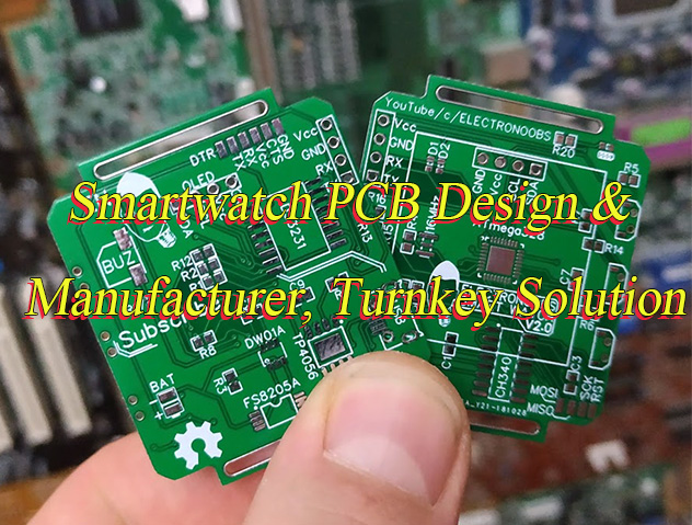
What is smartwatch PCB? Let’s explore definition, material selection, technical spec and guideline, production process and cost for smartwatch PCB.
Are you worried about these questions?
- Does smartwatch excessive heat generation affect user experience due to conventional PCB’s inadequate heat dissipation?
- How to guarantee yield rate when ultra-thin design causes PCB deformation?
- Does metal casing signal interference and poor communication stability cause high return rates?
As a smartwatch PCB manufacturer, EBest Circuit (Best Technology) can provide you service and solution:
- Aluminum substrate triples thermal conductivity efficiency, dropping chip temperature by 15°C to eliminate thermal discomfort.
- 0.8mm metal substrate withstands 10,000-cycle flexural testing without cracking, combining slim profile with durability.
- Custom dielectric layer provides interference shielding, increasing Wi-Fi/Bluetooth signal strength by 20%.
Welcome to contact us if you have any smartwatch PCB: sales@bestpcbs.com.
What is Smartwatch PCB?
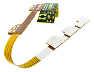
Smartwatch PCB utilize rigid-flex technology to create high-density miniature circuit boards. Their core function is to integrate electronic components, including main control chips, biosensors, and wireless communication modules, within extremely limited space (typically less than 30mm in diameter).
Polyimide flexible substrates enable dynamic bending adaptation to the wrist’s motion, while nanoscale anti-corrosion coatings ensure IP68 waterproof and sweatproof performance. These designs guarantee stable operation across temperatures ranging from -40°C to 85°C and support up to 100,000 bending cycles, meeting durability demands for wearable devices.
Which Material is Best for a Smartwatch PCB?
Polyimide (PI) Substrate Flexible and Lightweight Preferred
- Adopts 25-50μm ultra-thin PI substrate with thickness equivalent to half a human hair diameter. Maintains elasticity from -20℃ to 120℃ and withstands 100,000 bending cycles at 5mm radius while maintaining insulation resistance above 10¹⁰Ω, far exceeding conventional FR-4’s 10⁸Ω.
- Combined with 12μm rolled copper foil and arc-transition wiring design, achieves 0.07mm total thickness and weighs only 0.5g (approximately a snowflake’s weight). Perfectly suited for curved-fit and miniaturization needs of smartwatches. A flagship smartwatch achieved 40% weight reduction and 30% improvement in wear comfort compared to previous models using PI substrate.
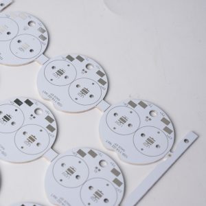
Aluminum Substrate High-Efficiency Thermal Management Core
- Features 1.5-2.0mm thick aluminum base layer with thermal conductivity of 200-250W/m·K, 250 times higher than FR-4’s 0.8W/m·K. Utilizes micro-via thermal conduction patent to rapidly transfer heat from high-power components (e.g., LEDs/power modules) to the aluminum base, reducing junction temperature by 25-40℃ and extending device life.
- Commonly used in power management modules or high-power chip cooling for smartwatches. A brand smartwatch achieved 60℃ continuous operation without thermal overload and 30% improvement in heat dissipation efficiency using aluminum substrate.
Ceramic Substrate High Wear Resistance and Signal Stability
- Zirconia ceramic with Mohs hardness 8.5 (close to sapphire’s 9) offers wear resistance, skin-friendliness, and hypoallergenic properties. Its dielectric constant is three times that of sapphire, reducing signal transmission loss by 50%. Nano-powder molding technology enables 0.03mm ultra-thin substrate supporting wireless charging and 5G signal penetration.
- Commonly used in smartwatch cases, back covers, or high-frequency modules. A brand smartwatch achieved 20% improvement in signal sensitivity, threefold improvement in wear resistance, and two-year extension in service life using ceramic back cover.
Halogen-Free FR-4 Environmental and Cost Balance
- Uses phosphorus-based flame-retardant resin and alkali-free glass cloth, complying with EU REACH standards. Heavy metal content below 10ppm and no toxic gas emission during combustion.
- Commonly used in smartwatch mainboards or low-power modules, costing 15-20% less than aluminum substrate while maintaining traditional FR-4’s insulation performance and processing maturity. A children’s smartwatch achieved no allergic reactions in skin irritation tests using halogen-free FR-4.
Smart Watch PCB Technical Specification
| Parameter Item | Specific Requirements |
| Board Material Type | High-Tg FR4 (Tg≥170℃) or High-Frequency Material (for RF areas) |
| Dielectric Constant (1GHz) | εr = 4.2±0.1 (core layer) |
| Loss Tangent (1GHz) | tanδ ≤ 0.02 |
| Total Thickness | 0.8±0.1mm (including copper foil and solder mask) |
| Minimum Core Thickness | ≥0.1mm |
| Copper Foil Thickness (Outer/Inner Layer) | Outer: 18μm Hoz; Inner: 12μm |
| Minimum Trace Width/Spacing | 60μm/60μm (L/S) |
| Laser Drill Hole Diameter | ≥0.1mm (mechanical drill) / ≥0.075mm (laser drill) |
| Via Annular Ring Width | ≥0.075mm |
| BGA Area Pad Diameter | ≥0.25mm (pitch 0.4mm) |
| Solder Mask Bridge Width | ≥0.05mm |
| Solder Mask Opening Expansion | Single side 0.05mm (pad) |
| Character Line Width | ≥0.12mm |
| Surface Finish Type | ENIG (Ni thickness ≥3μm, Au thickness ≥0.05μm) |
| Pad Coplanarity | ≤15μm (local area) |
| RF Differential Impedance (e.g., Bluetooth antenna) | 90Ω±7% (with complete GND reference layer) |
| High-Speed Signal Single-Ended Impedance | 50Ω±10% |
| Thermal Via Density (CPU area) | ≥4 vias/mm² (hole diameter 0.2mm) |
| Copper Thickness (Thermal Dissipation Area) | Outer: 2oz, Inner: 1oz |
| Ionic Contamination Level | ≤1.56μg/cm² NaCl equivalent |
| Thermal Stress Test | No delamination after 3 times 288℃ reflow soldering |
| Gold Plating Thickness (charging/data interface) | ≥0.2μm Au (Ni underlayer ≥3μm) |
| Mating/Unmating Life | ≥5000 cycles |
| Electrical Test Coverage | 100% Net |
| Flying Probe Test Minimum Pitch | ≥0.15mm |
| Flex Area (if applicable) | Bend radius ≥5mm, cycle life ≥10000 times |
| Waterproof Sealing Area | Solder mask opening width ≤0.1mm |
| Process Edge Width | ≥5mm (per side) |
| Mark Point Quantity | Diagonal ≥2 points, spacing ≥70% of board length |
How to Design a Smartwatch PCB Board?
Below is a guide to smartwatch PCB design:
1. Requirement Analysis and Function Definition
- Core Function Clarification: Define essential modules including heart rate monitoring, GPS positioning, Bluetooth/Wi-Fi communication, NFC payment, motion sensors (accelerometer/gyroscope), display drivers, and haptic feedback.
- Quantified Performance Metrics: For example, battery life ≥3 days (typical usage), charging time ≤2 hours, operating temperature range -20℃~60℃, waterproof rating IP68.
- User Scenario Alignment: Optimize designs for sports, medical, and daily wear scenarios—e.g., enhance GPS accuracy and real-time heart rate monitoring for sports, meet biocompatibility standards for medical use.
2. Component Selection and Integration Optimization
- Main Controller Chip: Prioritize low-power SoCs (e.g., ARM Cortex-M series) integrating GPU, memory controller, and PMU to reduce external components.
- Sensor Integration: Use modular designs (e.g., 6-axis IMU, optical heart rate sensors) while avoiding magnetic interference sources (speakers/motors) in layout.
- Power Management Solution: Adopt high-efficiency DC-DC converters (e.g., Buck converters) and LDOs, paired with battery protection chips (overcharge/discharge/short-circuit protection).
- Wireless Module Layout: Keep Bluetooth/Wi-Fi antennas away from metal shields; use FPC flexible antennas or ceramic antennas to ensure signal integrity.
3. PCB Layout and Stack-up Design
- Layer and Material Selection: Recommend 6–8-layer boards (2 signal layers + 2 power layers + 2 ground layers) with FR-4 or high-frequency substrates (e.g., Rogers 4350B); surface finish ENIG for soldering reliability.
Layout Principles:
- Module Partitioning: Separate digital circuits (MCU, memory), analog circuits (sensors, audio), and power circuits to minimize crosstalk.
- Critical Path Optimization: High-speed signals (e.g., USB, MIPI DSI) ≤5cm trace length, differential pairs (100Ω±10% impedance), avoid via cross-split planes.
- Component Placement: Place heat-generating components (PMUs, power amplifiers) near heat-dissipation zones; sensitive devices (crystals, ADCs) away from noise sources.
- Ground Plane Partitioning: Single-point connection for digital/analog grounds via beads or 0Ω resistors to reduce ground bounce noise.
4. Power Management Design
- Multi-Voltage Domain Management: Core MCU voltage (1.8V/3.3V), sensor power (1.2V/1.8V), display backlight (5V/12V) via LDO/DC-DC conversion.
- Low-Power Design: Implement DVFS, sleep modes (<10μA standby current), and power sequencing control.
- Battery Protection: Integrate over-voltage/under-voltage circuits with Li-ion protection ICs (e.g., DW01A) to prevent aging or safety issues.
5. Signal Integrity and EMI/EMC Design
- Impedance Control: Match 50Ω/100Ω impedance for high-speed lines via stack-up calculations (trace width/spacing).
- Crosstalk Suppression: Shield sensitive signals (analog sensors) or use ground wraps; maintain ≥3× trace width spacing.
EMC Protection:
- Add TVS diodes (ESD protection) to input ports (e.g., charging ports).
- Use π-type filters (capacitor-inductor-capacitor) for RF modules to reduce conducted/radiated noise.
- Shield high-frequency modules (Wi-Fi chips) with metal covers to minimize EMI leakage.
5. Thermal Management Design
- Thermal Path Planning: Under high-power chips (MCUs, PMUs), deploy large copper pads connected to metal enclosures via thermal pads/grease.
- Thermal Simulation: Validate junction temperature ≤125℃ (chip safety) and surface temperature ≤45℃ (human contact safety) using tools like ANSYS Icepak.
- Passive Cooling: Add graphene heat sinks on PCB backsides; optimize airflow channels (e.g., watch case vents).
6. Manufacturability and Reliability Design
- DFM/DFA Rules: Component spacing ≥0.2mm (avoid solder bridges); IPC-compliant pads (e.g., QFN thermal pads); SMT-compatible packages (0402/0603).
- Reliability Testing: Validate PCB durability via thermal cycling (-40℃~85℃), vibration (IEC 60068-2-6), and salt spray (ASTM B117) tests.
- BOM Optimization: Reduce material types (unify capacitor/resistor brands); prioritize automotive/industrial-grade components.
7. Testing and Verification Process
- Prototype Validation: Test functions (button response, display brightness), power (current consumption, voltage ripple), and signals (eye diagram, timing) on engineering samples.
- EMC Certification: Meet standards like CISPR 32 (radiated emissions) and IEC 61000-4-2 (ESD immunity).
- Mass Production Inspection: Perform AOI, X-ray, and functional sampling on batched PCBs to ensure consistency.
8. Packaging and Protection Design
- Waterproofing: Apply conformal coating (silicone resin) to PCB edges; use waterproof sealants on connectors; add O-rings between cases and PCBs.
- Shock Resistance: Secure critical components (crystals, connectors) with adhesive to prevent vibration-induced detachment.
- User Interface Protection: Add ESD circuits to touchscreens; use metal dome switches for button interfaces to enhance contact reliability.
How to Manufacture a Smart Watch PCB?
1. Design Output
- Use Altium Designer/OrCAD to complete circuit design, must include heart rate monitoring, GPS positioning, and other modules.
- Gerber files contain signal layer/power layer/ground layer layouts, Excellon drilling files, and solder mask/silkscreen data.
- BOM (Bill of Materials) must specify component models, package dimensions, and procurement channels to ensure traceability.
- Perform DFM (Design for Manufacturing) verification during the design phase to avoid issues like excessively small line widths/spaces or defective pad designs.
2. Substrate Preparation
- For high-frequency scenarios, use Rogers 4350B or Panasonic Megtron 6; FR-4 is used for cost-sensitive applications.
- Copper-clad laminate cutting accuracy ±0.1mm, using automatic cutting machines to avoid burrs.
- Copper thickness 1oz (0.035mm) or 2oz (0.07mm); high-power areas use 2oz for enhanced heat dissipation.
- Clean substrates to remove oil and oxidation layers, ensuring adhesion for subsequent processes.
3. Inner Layer Circuit Fabrication
- Use LDI (Laser Direct Imaging) technology for pattern transfer with ±5μm accuracy, avoiding film exposure errors.
- UV exposure energy 80-120mJ/cm², developer concentration 10-15% Na₂CO₃, temperature 30-35°C.
- Etching solution uses acidic copper chloride, temperature 45-50°C, speed 1.2-1.5m/min, ensuring neat line edges.
- AOI (Automated Optical Inspection) testing uses 3D imaging technology with ±10μm accuracy to detect opens, shorts, and copper deficiencies.
4. Lamination Molding
- Symmetrical stack-up design (e.g., core board + prepreg + copper foil) to avoid warping after lamination.
- Vacuum lamination temperature 180-200°C, pressure 300-400psi, time 90-120 minutes.
- Prepreg uses high-Tg material (e.g., Shengyi S1141) to prevent delamination during reflow soldering.
- Post-lamination X-ray inspection for interlayer alignment accuracy ≤50μm.
5. Drilling
- Laser drilling uses CO₂ laser, hole diameter ≤0.1mm, suitable for HDI (High Density Interconnect) board blind/buried vias.
- Mechanical drilling uses minimum 0.2mm drill bit, speed 80,000rpm, feed rate 0.5m/min.
- Plasma etching after drilling to remove debris, ensuring clean hole walls.
- Positioning holes use pin alignment with ±0.05mm accuracy for subsequent assembly alignment.
6. Hole Metallization
- Chemical copper deposition thickness 1-2μm to form a conductive base; electroplated copper thickness 25-30μm to avoid voids.
- Electroplating uses pulse power, backlight inspection ≥8 levels to ensure uniform hole plating.
- Hole wall roughness Ra ≤2μm to reduce signal transmission loss.
7. Outer Layer Circuit
- Outer layer pattern transfer uses LDI technology with ±5μm accuracy to ensure circuit precision.
- Secondary AOI testing uses high-speed line scanning to detect line width/space deviations and copper deficiencies.
- Outer layer circuits undergo anti-oxidation treatment (e.g., nickel-gold plating) to prevent oxidation affecting soldering.
- Plasma cleaning of circuit edges enhances solder mask adhesion.
8. Solder Mask & Silkscreen Printing
- Solder mask uses liquid photoimageable ink (e.g., Taiyo PSR-4000), coating thickness 20-30μm, soldering temperature resistance 260°C.
- Exposure uses UV LED with 300-500mJ/cm² energy to ensure complete ink curing.
- Silkscreen printing uses white ink with font height ≥0.2mm for readability.
- Solder mask opening accuracy ±0.05mm to avoid pad misalignment.
9. Surface Finish
- ENIG (Electroless Nickel Immersion Gold) uses 4-6μm nickel + 0.05-0.1μm gold to enhance solder reliability.
- OSP (Organic Solderability Preservative) uses organic film with 0.2-0.5μm thickness, cost-effective but with a 6-month shelf life.
- Post-surface finish, perform solderability testing (e.g., wetting balance) to ensure welding performance.
- High-reliability products use ENEPIG (Electroless Nickel Electroless Palladium Immersion Gold) for enhanced high-frequency signal stability.
10. Testing & Depanelization
- Electrical testing uses flying probe (±0.02mm accuracy) or bed-of-nails (contact resistance ≤0.1Ω) to verify circuit connectivity.
- Impedance testing uses TDR (Time Domain Reflectometry) to ensure high-frequency signal line impedance matching (e.g., Bluetooth antenna ±10%).
- V-CUT depanelization uses milling cutter with ±0.1mm accuracy to avoid burrs affecting assembly.
- Post-depanelization, perform ionic contamination testing (e.g., ROS-120) to ensure cleanliness.
11. Final Inspection & Packaging
- Visual inspection uses AOI or manual methods to detect defects like scratches, deformation, or color discrepancies.
- Vacuum moisture-proof packaging uses aluminum bags + desiccant with humidity ≤5% to prevent oxidation.
- Packaging includes production date, batch number, and environmental compliance markings (e.g., RoHS) for traceability.
- Final products undergo environmental testing (e.g., high-temperature/humidity, thermal shock) to ensure reliability.
How Much Does it Cost to Make a Smartwatch PCB?
The manufacturing cost of smartwatch PCBs is strictly affected by the number of layers, materials, and process complexity, and the price is calculated based on the unit price of an order of 1,000 pieces: the basic model uses a 4-layer FR-4 board and conventional process, with a single board cost of approximately $8-15, suitable for entry-level smartwatches; the mid-to-high-end model is upgraded to a 6-8-layer HDI board and uses high-frequency materials, with the cost climbing to $25-50, which must meet the high-precision requirements of Bluetooth/Wi-Fi/GPS multi-mode radio frequency.
If the model uses a flexible PCB + ultra-thin design combined with laser drilling and immersion gold technology, with a unit price of up to $60-120. Its core cost drivers are concentrated on ±5% impedance control accuracy and miniaturized component placement technology. It is worth noting that if the order volume is less than 1,000 pieces, the unit price will increase by 30%-50%, which further highlights the key balancing role of precision manufacturing technology and large-scale production in cost control.
Why Choose EBest Circuit (Best Technology) as Smartwatch PCB Manufacturer?
Reasons why choose us as smartwatch PCB manufacturer:
- 19-Year Expertise Vault: 19 years of PCB manufacturing expertise and error database-driven risk prediction reduce rework costs by 5%-10% per order, turning experience into tangible savings.
- Global Certification: ISO 19001, IATF 16949 automotive-grade, medical-grade, and RoHS, which guarantee compliance with global market entry requirements, enabling seamless international market access.
- Free DFM Technology: Complimentary Design for Manufacturability analysis identifies design flaws and process risks upfront, cutting mass production preparation time by 30% and costs by 20%, ensuring design excellence.
- Full Turnkey Solution: Integrated PCB fabrication, component sourcing, SMT assembly, and functional testing streamline supply chain management by 40%, allowing clients to focus on core innovation.
- 24 Hours Rapid Prototyping: 24-hour rapid prototyping for urgent orders, compressing design-to-prototype cycles to 1 day, accelerating product iteration, and delivering “first-mover” commercial advantage.
- Revolutionary Cost Optimization: Leverage intelligent material selection and process streamlining to achieve 15%-30% single-board cost reduction, enabling price competitiveness across entry-level to flagship smartwatch segments and securing high-value market share.
- Unmatched Delivery Reliability: 99.2% on-time delivery rate powered by AI-driven smart scheduling and global supply chain collaboration, eliminating delivery risks and ensuring production peace of mind.
- Strict Quality Commitment: 100% batch inspection coverage with AOI/X-Ray/functional testing, achieving 99.9% yield rate and superior performance consistency, far exceeding industry standards.
- RF Expertise for Multi-Mode Connectivity: Master HDI laser drilling, immersion gold, and ±3% impedance control to support Bluetooth/Wi-Fi/GPS multi-mode RF demands, enhancing signal integrity by 20% and outperforming competitors.
How to Start a Smart Watch PCB Project?
Quotation Checklist for Smartwatch PCB Project:
1. PCB Specifications
- Layer count (e.g., 4/6/8 layers)
- Material type (FR-4, HDI, or flexible PCB)
- Board thickness and impedance control requirements.
2. Components & Assembly
- BOM (Bill of Materials) cost for ICs, sensors, and connectors.
- SMT (Surface Mount Technology) assembly fees.
- Testing and quality control charges.
3. Design & Engineering
- Schematic and layout design fees.
- RF/wireless module integration costs (Bluetooth/Wi-Fi/GPS).
4. Production & Logistics
- Prototyping cost (e.g., 5-10 boards).
- Bulk production MOQ (Minimum Order Quantity) and unit price.
- Shipping and import duties (if applicable).
5. Additional Services
- Certification compliance (FCC, CE, etc.).
- IP protection (NDA or custom firmware costs).
Welcome to submit your Gerber files to get a quote for you now: sales@bestpcbs.com.
You may also like


Tags: smartwatch PCB