

High speed board design is the process of creating printed circuit boards that handle signals with extremely fast rise times and high data rates. Impedance, crosstalk, and signal reflections become critical factors, so every layout detail matters.
Unlike standard PCBs, high speed boards require controlled impedance traces, precise layer stack-ups, and low-loss materials. Designers plan the stack, routing, and grounding from the start to maintain clean waveforms and stable timing. The goal is to move large amounts of data quickly while preserving signal integrity and meeting strict electromagnetic compatibility standards.
Do you have the following questions about high-speed PCB design?
- What are the consequences of impedance mismatch in high-speed PCB design?
- What are the effects of close traces in high-speed PCB design?
- How can a PCB both be affected by and generate interference?
- How should return current paths be considered in high-speed PCB design?
- This can cause signal reflections and waveform distortion (such as overshoot and ringing), leading to data errors and timing errors, seriously impacting system stability.
- This primarily causes crosstalk, which is electromagnetic coupling interference between adjacent signal lines. This can contaminate signal quality, affect impedance, and exacerbate electromagnetic radiation (EMI) issues.
- High-speed signals on PCBs are inherently high-frequency noise sources that can emit electromagnetic interference (EMI) through radiation or conduction. Furthermore, external electromagnetic fields can couple onto PCB traces, making them receptors for interference.
- For high-speed signals, a complete reference plane (ground or power plane) must be provided close to the signal lines to ensure a continuous, low-inductance return path and avoid plane segmentation. When changing layers, ground vias should be added next to signal vias to provide a path for return current.
BEST Technology ensures high-frequency, high-speed performance and reliability of PCBs through comprehensive material, design, and process control.
We test material Dk values to provide scientific stackup and linewidth solutions, and rigorously control the production process to ensure impedance matching.
We also provide Design for Factoring (DFM) analysis to proactively mitigate crosstalk and EMI risks, and offer a variety of high-frequency material options to meet EMC requirements.
We also utilize a symmetrical stackup design with strict control over alignment and hole metallization processes to ensure a complete and reliable return path.
What is a high speed PCB?
High speed PCBs are designed specifically for high-speed digital circuits. They are primarily optimized for high-frequency signals (typically 100MHz to several GHz) and high data rates (such as PCIe 4.0, which reaches 16Gbps). Their design must address transmission line effects such as signal reflection, crosstalk, and impedance matching.
High-speed PCBs have the following core features:
1. Signal Integrity Control:
- Differential signaling, impedance matching (e.g., 50Ω or 100Ω), and shielded grounding techniques are used to reduce signal distortion.
- Electrical rule-driven routing simultaneously calculates overshoot and crosstalk, outperforming traditional physical rule-driven routing.
2. Materials and Processing:
- High-frequency laminates (such as Rogers and Isola FR4 high-speed grades) are used to minimize the frequency variation of dielectric loss (Df) and dielectric constant (Dk).
- Copper foil roughness must be extremely low (e.g., HVLP type), and routing accuracy must reach micron levels.
3. Thermal Management and EMC:
- Multi-layer board design optimizes heat dissipation paths and keeps power and ground planes close together to reduce noise.
- Verify electromagnetic compatibility using simulation tools (such as Ansys HFSS).
4. Strict Routing Rules:
- Shorten critical signal paths (such as clock lines), avoid right-angle routing, and use differential pair routing.
- Multi-layer board design provides a complete ground plane to reduce electromagnetic interference (EMI).
5. Power Integrity (PI):
- Optimize the power distribution network (PDN), reduce power supply noise, and use decoupling capacitors and low-impedance power planes.
Typical Application Scenarios:
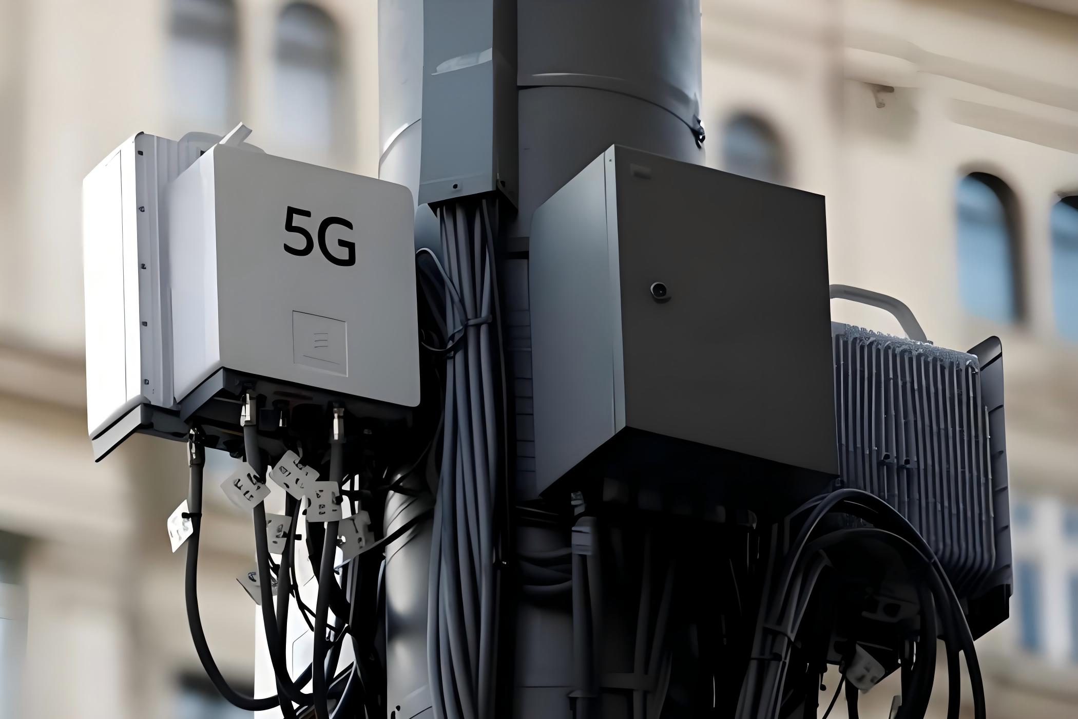
- 5G communications equipment
- High-speed data converters (ADC/DAC)
- Servers and high-end computing hardware
- Radar and RF systems
What makes high speed boards different from standard PCBS?
The main differences between high-speed PCBs and standard PCBs (ordinary PCBs) lie in design requirements, material selection, and manufacturing processes. The specific differences are as follows:
- Design Principles
High-speed PCBs prioritize signal integrity (SI), electromagnetic compatibility (EMC), and power integrity (PI). They employ differential pair routing and impedance matching techniques to minimize signal loss. Standard PCB design focuses primarily on circuit functionality, with lower requirements for signal integrity and EMI.
- Material Selection
High-speed PCBs often utilize substrate materials with low dielectric constant (Dk) and low loss (e.g., FR-4, Rogers), and may use thicker copper foil to increase current carrying capacity. Standard PCBs typically use lower-cost substrates such as FR-2/3 and thinner copper foil.
- Manufacturing Process
High-speed PCBs require precise control of trace width and spacing, and employ blind and buried via technology to optimize signal transmission. Standard PCB manufacturing processes are relatively simple, prioritizing a balance between cost and functionality.
- Stackup Structure
High-speed PCBs feature multi-layer designs (six or more layers) with integrated ground and power planes to reduce EMI. Standard PCBs typically have two to four layers, and power and ground planes may be incomplete.
- Performance Requirements
High-speed PCBs require rigorous testing to verify signal timing performance and prioritize thermal management to maintain stability in high-temperature environments. Standard PCBs have lower requirements for heat dissipation and signal integrity.
What is high speed PCB design?
High-speed PCB design is a circuit board design technology designed for high transmission rates and high signal frequencies. It is primarily used in high-speed digital signal transmission scenarios and must address issues such as signal reflection, crosstalk, and electromagnetic interference.
Through techniques such as impedance matching, differential signal design, and layered routing, signal stability is ensured during transmission, preventing distortion and interference.
Key Technical Points:
- Impedance Matching: aligning transmission line impedance with terminal impedance to reduce reflections;
- Differential Signal Design: utilizing differential pair transmission to reduce crosstalk;
- Layered Routing: optimizing signal paths through a multi-layer structure to reduce crosstalk;
- Electromagnetic Compatibility (EMC): minimizing the effects of electromagnetic radiation through shielding and grounding.
How to follow high speed board design guidelines?
Follow these steps to avoid common issues and create stable boards.
- 1. Start With a Clear Schematic
Keep signal paths short and direct. Identify clocks and other critical nets early. Mark high speed nets clearly for the layout stage.
- 2. Define the Stack-Up First
Determine layer sequence, dielectric thickness, and copper weight. Lock these details before routing. Controlled impedance depends on accurate stack-up data.
- 3. Control Trace Impedance
Calculate trace width and spacing for each layer. Use microstrip or stripline geometry as required.
- 4. Keep Return Paths Clean
Always provide a continuous ground plane. Avoid splits or gaps under high speed traces. A clean return path limits radiation and keeps impedance stable.
- 5. Minimize Crosstalk
Separate aggressive signals from sensitive ones. Increase spacing between differential pairs when possible. Route high speed lines over solid reference planes.
- 6. Reduce Via Count
Every via adds inductance and reflection. Use them only when needed. If a via is required, back-drill or use blind/buried vias to shorten the stub.
- 7. Plan Power Delivery
Place decoupling capacitors close to each IC pin. Use multiple values to handle different frequency ranges. Ensure the power plane is wide and continuous.
Transitioning between them carefully ensures the design remains stable from concept to production.
What are the key considerations for designing a high speed PCB?
What is the frequency of a high-speed PCB?
The operating frequency range for high-speed PCBs typically starts at 300MHz and can reach tens of GHz. Depending on the application scenario and technical requirements, these frequency bands can be categorized into the following typical bands:
- 1. High-frequency starting point: 300MHz-1GHz (commonly used in wireless communications, RF modules, and other applications)
- 2. High-frequency/RF range: Above 1GHz (Wi-Fi, Bluetooth, 5G, and other applications)
- 3. Microwave band: 300MHz-30GHz (including 5G Sub-6GHz, satellite communications, radar, and other applications)
- 4. Millimeter-wave band: Above 30GHz (such as 5G indoor millimeter-wave applications)
What material is used for high speed PCB design?
Material choice is critical. Standard FR-4 can work up to a point, but its loss and dielectric constant may not stay stable at very high frequencies.
Popular options include:
- Rogers laminates with low dielectric loss and tight Dk control.
- Isola high speed materials for stable performance across temperature.
- Megtron series for ultra-low loss in 10 Gbps and faster systems.
When selecting materials, consider cost, availability, and the required frequency range.
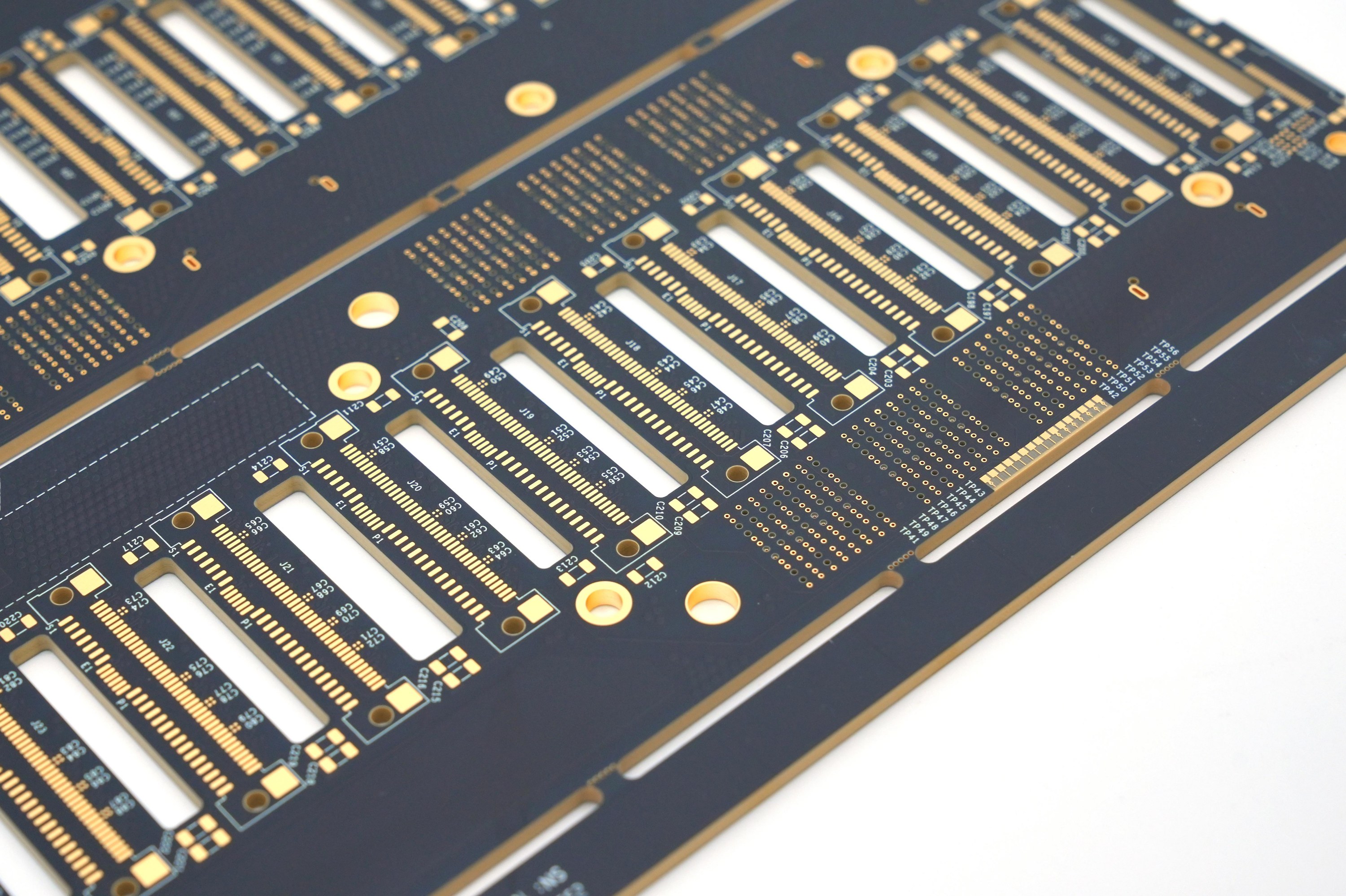
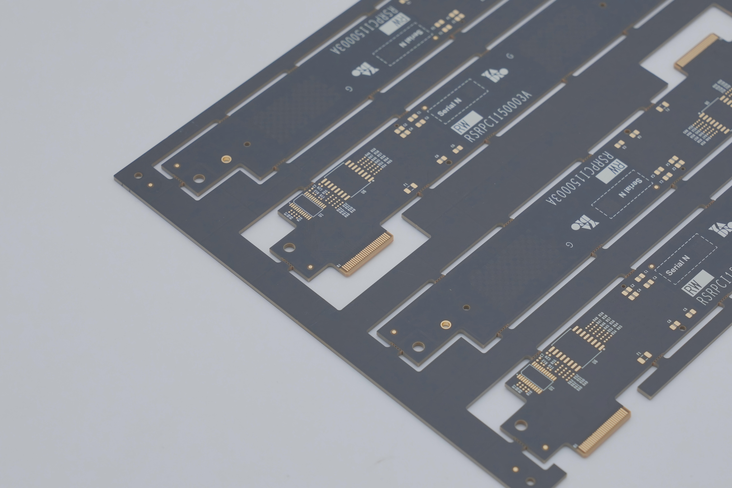
What layer stack-up works for high speed boards?
High-speed circuit boards typically use a six-layer stackup, a design that balances signal integrity, power management, and electromagnetic shielding requirements. A typical high speed PCB might use:
- Top signal layer for components and short traces.
- Ground plane directly beneath for clean return paths.
- Internal signal layers sandwiched between power and ground.
- Bottom signal layer for low-speed connections.
For higher-frequency applications (such as FPGAs and high-end CPUs), eight or more layers may be used to support multiple power domains and complex bus designs.
How to control EMI in high-speed design?
Controlling EMI in high-speed designs requires multiple approaches, including device selection, layout optimization, and signal processing. Careful layout reduces EMI and keeps devices compliant with regulations.
Here are proven methods:
- Continuous Ground Planes: Provide a low-impedance return path to reduce loop area.
- Short Traces: Keep high speed lines as short as possible to limit radiation.
- Proper Termination: Use series or parallel termination to prevent reflections.
- Shielding: Place ground pours or metal shields near critical circuits.
- Differential Pairs: Route balanced differential signals to cancel magnetic fields.
Combining these strategies lowers emissions and helps pass EMC tests on the first attempt.
Conclusion:
EBest Circuit (Best Technology) Co., Ltd. brings nearly two decades of expertise in creating low-loss, controlled-impedance boards for 5G, networking, medical, and advanced consumer electronics. For expert support or to request a quote, contact sales@bestpcbs.com
You may also like


Tags: high speed board, high speed board design guidelines, high speed boards, high speed design guidelines, high-speed design