

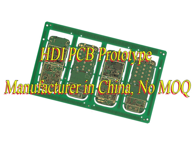
As an HDI PCB manufacturer, EBest Circuit (Best Technology) understands the importance of reliable, high-quality HDI PCBs for modern electronics. The core content of this blog revolves around the definition, features of the HDI board, and the HDI PCB manufacturing process.
Some customers face the following issues when doing the HDI printed circuit boards project with their HDI PCB manufacturers. Are you also dealing with these frustrating problems?
- Extended lead times and the delayed delivery time from a certain HDI PCB manufacturer?
- High cost and its impact on some cost-sensitive projects?
- Product defect due to poor manufacturing precision?
- There are some difficulties in customizable design, size, material, and other aspects, so it is difficult to meet the specific needs of your orders?
Here’s our game plan for dealing with those tricky problems.
- Boost manufacturing process and shorten delivery schedule: The production efficiency can be improved by elevating the HDI PCB manufacturing process and using automatic devices. Finally, to shorten the entire fabrication lead time.
- Optimize the cost structure and improve the cost efficiency: We can lower the unit cost by standard design, mass production, and material selection optimization.
- Increase the manufacturing precision and improve product quality: Adopt high-precision equipment, such as a laser drilling machine, AOI inspection equipment, and a rigorous quality control process to ensure product consistency.
- Boost customizable capability: provide the tailored manufacturing service according to customers’ Gerber files and needs.
As an ODM & OEM HDI circuit boards manufacturer, we have our own high density interconnect PCB factory in China, and we have been selling high-density PCBs in a perfectly competitive market for over 19 years. Our customer vary from countries to countries. Last year, our biggest selling volume is to the USA, Germany, and Israel, and others. We have abundant experience in solving different issues for customer’s projects. If you need to find a reliable manufacturers for HDI PCB fabrication services, just make contact with us via sales@bestpcbs.com.

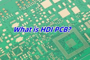
What is HDI PCB?
The full name of HDI PCB is high-density interconnect PCB. Put it simply, it refers to a multilayer PCB produced using build-up techniques and microvias. In simple terms, it starts with a core board—with or without plated through holes (PTH)—made by conventional methods. Fine circuits and microvias are then added to the outer layers to create build-up layers, ultimately forming a multilayer board.
To better understand how HDI PCBs achieve high-density interconnections, it’s useful to first look at the different types of vias used in these boards.

Via hole: It is a general term for all layer-to-layer holes, including Through Holes, Blind Vias, Buried Vias, and Microvias.
Microvia: In the PCB industry, any hole with a diameter smaller than 150 µm (6 mil) is classified as a microvia. It is very small via for HDI PCBs, can be blind, buried, or through.
Buried via: A buried via is located within the inner layers and is typically invisible in the finished PCB. Compared with through-holes, its main advantage is that it does not occupy surface space, allowing more components to be placed on the PCB’s surface.
Blind via: A blind via is visible on the finished PCB but only from one side. Unlike through-holes, which are visible from both the top and bottom, blind vias allow routing underneath the via location while saving surface area for components.
Through Hole: A through hole is a type of via hole that passes through the entire PCB. In other words, all through holes are via holes, but not all via holes are through holes. Via holes can also include blind vias and buried vias, which only connect some layers of the PCB rather than the entire board, allowing for higher-density layouts. When a through hole is plated with copper, it is called a PTH and is used for electrical connections. If it is not plated, it is called an NPTH and serves mainly mechanical purposes.
| Via Type | Typical Min. Diameter | Layer Connection | Common Use Case |
|---|---|---|---|
| Via Hole | N/A | Any layers | General layer-to-layer interconnection |
| Microvia | ≤ 150 µm (6 mil) | Outer to inner (1 layer) | High-density routing |
| Blind Via | 75–200 µm | Outer to inner (partial) | Space-saving design |
| Buried Via | 100–200 µm | Inner to inner only | Inner layer connection |
| Through PTH | ≥ 200 µm | All layers | Signal & power transfer |
| Through NPTH | ≥ 200 µm | No electrical connection | Mechanical fixing |
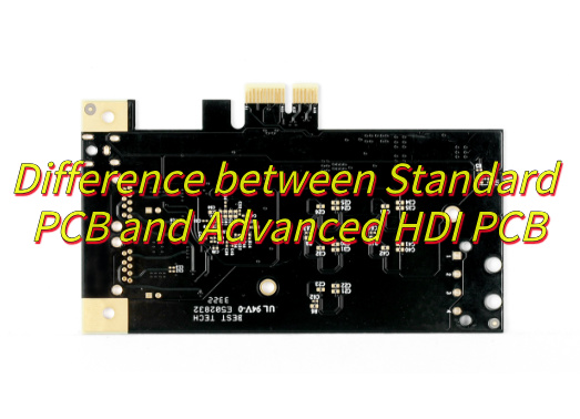
What is the Difference Between HDI PCB and Conventional PCB?
1. Layer Structure
- HDI PCB: Uses multiple build-up layers with microvias, blind vias, and buried vias, allowing higher interconnect density in a compact design.
- Conventional PCB: Relies on through-hole vias across the entire board with simpler stack-up, suitable for less dense layouts.
2. Fine Line Width and Spacing
- HDI PCB: Supports ultra-fine lines and spaces, often down to 50–75 microns, enabling high-density routing.
- Conventional PCB: Uses wider traces and spacing, which limits circuit miniaturization.
3. Process Technology
- HDI PCB: Requires laser drilling, sequential lamination, and via-in-pad technology for advanced designs.
- Conventional PCB: Uses mechanical drilling and traditional lamination, easier to fabricate for general applications.
4. Base Materials
- HDI PCB: Employs high-performance laminates with low Dk/Df for better high-frequency performance and thermal stability.
- Conventional PCB: Commonly made with standard FR4, good enough for most consumer and industrial electronics.
5. Manufacturing Cost
- HDI PCB: Higher cost due to extra processes, fine features, and strict material requirements.
- Conventional PCB: More cost-effective, especially for low-to-medium complexity products.
6. Application Scenarios
- HDI PCB: Found in smartphones, tablets, medical devices, automotive electronics, and aerospace where size and performance are critical.
- Conventional PCB: Used in home appliances, industrial controls, and products that don’t need very high density.
Structural Characteristics of HDI Blind Vias
High-Density Interconnect (HDI) PCBs are characterized by their use of blind vias, which connect outer layers to one or more inner layers without passing through the entire board. The structural configuration of HDI boards is typically described using a notation like a+N+a or a+N+N+a, where each element represents a specific part of the board:
- “a” – Build-up Layer: These are the additional layers added on top of the core to achieve higher wiring density. Each build-up is considered a stage: a single build-up is first-order, two sequential build-ups are second-order, and three build-ups constitute third-order.
- “N” – Core Layer: This is the central layer of the PCB that provides mechanical support and basic circuitry.
Some common HDI structures include:
- 1+N+1: One build-up layer on each side of the core.
- 1+N+N+1: One build-up on each side with an additional core layer in the middle.
- 2+N+2: Two build-up layers on each side of the core.
- 2+N+N+2: Two build-up layers on each side with an extra core layer in between.
- 3+N+3: Three build-up layers on each side of the core.
- 3+N+N+3: Three build-up layers on each side with an extra core layer in the center.
These configurations allow for greater routing density, smaller via sizes, and more compact designs. The use of blind vias reduces signal loss, minimizes board thickness, and enables complex circuitry integration without increasing the overall PCB size. By carefully selecting the build-up and core combination, designers can optimize signal integrity and maintain mechanical stability in advanced electronic devices.

Where to Get HDI PCB Manufacturer in China for PCB Fabrication and Assembly?
China is renowned for its manufacturing capacity, offering a greater range of HDI PCB fabrication and assembly services. When looking for a reliable HDI PCB manufacturer, it’s important to understand the market landscape first.
HDI Boards Market Overview
HDI PCB factories in China are concentrated in several key regions:
- Shenzhen and Guangdong Province: Known for high-tech electronics and fast-turn advanced HDI PCB manufacturing.
- Jiangsu and Zhejiang Province: Strong in medium to large-scale production, including rigid-flex HDI PCB boards and multi-layer high density interconnect PCBs.
- Other regions: Specialized factories exist in cities like Shanghai, Tianjin, and Beijing, focusing on niche or high-end HDI PCB fabrication.
Channels to Get Original China HDI PCB Manufacturer
- Trade shows and electronics exhibitions – opportunities to see HDI PCB fabrication capabilities firsthand.
- Online B2B platforms and directories – such as Alibaba and Global Sources, offer a large range of manufacturers that provide HDI PCB assembly manufacturing and other services.
- Industry referrals and engineering networks – recommended by partners who have experience with hdi pcb electronics manufacturing.
Types of HDI PCB Manufacturers in China
- Professional HDI factories: Focus solely on HDI boards, often equipped with blind buried vias HDI PCB manufacturing, laser drilling, microvia technology, and sequential lamination. Ideal for high quality HDI PCB for electronics circuit boards and HDI PCB prototype manufacturing.
- General PCB manufacturers: Handle a variety of PCB types including HDI, but may have limitations on microvia precision or layer count. Suitable for medium-complexity designs and any PCB layer HDI manufacturers.
- OEM/ODM factories: Offer full services from design to assembly, including 3 step HDI PCB manufacturers or smart robot rigid-flex PCB board HDI board manufacturing, often supporting volume production for global electronics brands.
EBest Circuit (Best Technology) Advantages
When choosing HDI PCBs manufacturers, working with a PCB HDI company that addresses common customer pain points is key. EBest Circuit (Best Technology) stands out with:
- Advanced Manufacturing Capabilities: Supports multi-layer HDI PCB boards, HDI via PCB manufacturing, rigid-flex HDI PCB boards, and high density PCB designs.
- Original high density interconnect PCBs and SMT Factories: We have original HDI fabrication and SMT factories in China for PCB Fabrication and Assembly. And our ISO9001, IATF16949, ISO13485, and AS9100D certifications ensure strict process control and reliability in our own HDI PCB manufacturing and PCBA factories.
- Professional Engineering Support: HDI PCB design for manufacturability guide, layout optimization, and rapid prototyping minimize rework and maximize performance.
- Flexible Delivery: Solutions tailored for both small and large volume production, with reliable HDI PCB electronics manufacturing quality and reliable lead times.
In summary, finding the right China leading HDI PCB manufacturer for electronics industry involves understanding the regional landscape, knowing the types of factories available, and selecting a partner who can provide both technical expertise and dependable production. With advanced capabilities, rigorous quality control, and customer-focused service, EBest Circuit (Best Technology) ensures your high density interconnect PCB projects are executed efficiently, reliably, and with consistent high quality.
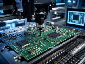
Step-by-Step HDI PCB Fabrication Process
EBest Circuit (Best Technology) follows a meticulous multi-stage approach to ensure the quality, reliability, and performance of every HDI board. Below is our 3 step HDI PCB fabrication process for your reference. As a 3 step HDI PCB manufacturer, EBest Circuit (Best Technology) leverages advanced laser drilling, sequential lamination, and microvia filling technologies to achieve high-density interconnects with exceptional precision.
Step 1: Material Preparation (Cutting)
Copper-clad laminates are cut into required panel sizes. Material properties such as thickness, CTE, and moisture absorption are carefully checked to ensure dimensional stability during subsequent processes. Pre-baking is often performed to remove absorbed moisture.
Step 2: Inner Layer Imaging
Photoresist is applied to the core, then exposed through a phototool to define fine circuit patterns. Strict control of exposure alignment and development ensures accurate line width and spacing.
Step 3: Automated Optical Inspection (AOI)
Inner layer circuits are inspected with AOI to detect defects such as opens, shorts, and over-etched lines. Any defects are repaired or flagged before proceeding to lamination.
Step 4: Lamination
The prepared inner layers are stacked with prepreg and copper foil, then laminated under high temperature and pressure. Vacuum lamination ensures strong bonding, minimal voids, and proper registration between layers.
Step 5: Copper Reduction (7–9 μm)
Controlled etching reduces copper thickness to the target range of 7–9 μm. This step is crucial for achieving fine line resolution and impedance stability in HDI structures.
Step 6: Laser Drilling (3–5 mil Holes)
Microvias are drilled using a CO₂ or UV laser. Hole diameters range from 3 mil to 5 mil depending on design requirements. Laser parameters are adjusted to ensure clean via walls and accurate depth control.
Step 7: Mechanical Drilling (Through-Holes, Aspect Ratio ≤5:1)
Through-holes are drilled mechanically, with the aspect ratio controlled to be ≤5:1. Drill bit wear and hole wall quality are closely monitored to avoid defects like burrs or smear.
Step 8: Electroless Copper Deposition
A thin conductive seed layer is deposited inside all drilled holes and via walls by electroless copper plating. This creates the foundation for subsequent electroplating.
Step 9: Hole Filling (Blind Via, ≤25 μm Copper Growth)
Blind vias are filled with conductive copper plating. Copper growth is controlled to ≤25 μm to maintain surface flatness, which is critical for further lamination and circuit imaging.
Step 10: Inner Layer Imaging (Repeated)
The next layer of circuitry is defined by repeating the photoresist coating, UV exposure, and development process. Alignment to buried features is precisely maintained.
Step 11: AOI
Each newly imaged layer undergoes AOI to confirm circuit accuracy before additional lamination steps.
Step 12: Lamination (Second Build-Up)
Another lamination cycle is carried out to stack additional layers. Temperature, pressure, and alignment are controlled to ensure reliability and dimensional stability.
Step 13: Copper Reduction
Etching is performed again to refine copper thickness to the design requirements, ensuring consistent trace definition.
Step 14: Laser Drilling
New microvias are laser-drilled to connect to the previously built-up layer. Registration accuracy is carefully monitored to avoid misaligned stacked vias.
Step 15: Electroless Copper Deposition
Copper seed layers are deposited again inside the new vias and on the panel surface to ensure complete metallization.
Step 16: Hole Filling
The newly created blind vias are filled and planarized, maintaining a smooth surface for further processing.
Step 17: Inner Layer Imaging (Third Build-Up)
The third sequence of inner layer circuit imaging is performed. High precision alignment is required as this is the final build-up before outer layer processing.
Step 18: AOI
AOI checks for defects such as misregistration, broken lines, and incomplete filling to guarantee layer reliability.
Step 19: Lamination (Final Build-Up)
All layers are consolidated in a final lamination cycle. Rigorous control of warpage and shrinkage is performed to meet high-density tolerances.
Step 20: Copper Reduction
The outer copper is reduced to the design thickness to prepare for outer layer circuit definition.
Step 21: Laser Drilling
Outer microvias are laser-drilled, connecting the final build-up layers to the outer copper surface. Alignment to internal features is verified.
Step 22: Mechanical Drilling
Final through-holes, tooling holes, and mounting holes are mechanically drilled with tight tolerance control.
Step 23: Electroless Copper Deposition
All newly drilled vias and holes receive electroless copper plating to establish a uniform conductive seed layer.
Step 24: Hole Filling
Any blind or buried vias requiring filling are processed and planarized to maintain surface flatness for solder mask application.
Step 25: Outer Layer Imaging
Outer layers are coated with photoresist and exposed with phototools to define final circuit traces and pads. Alignment is critical to match buried vias and inner layers.
Step 26: Etching
Unwanted copper is etched away, leaving the final outer layer circuitry with precise line width and spacing.
Step 27: AOI
Final AOI verifies the outer layer circuitry. Any defects are flagged, repaired, or scrapped based on quality requirements.
Step 28: Solder Mask Application
A solder mask layer is applied and imaged to protect circuits and define solderable pads. Adhesion, thickness, and registration are carefully checked.
Step 29: Silkscreen Printing
Component markings and reference designators are printed. Clarity, durability, and positioning are validated for assembly readability.
Step 30: Surface Finishing (ENIG / Gold Plating)
Surface finishes such as ENIG (Electroless Nickel Immersion Gold) are applied to exposed copper pads to improve solderability and oxidation resistance.
Step 31: Board Profiling
The panels are routed or V-scored into final board shapes. Dimensional accuracy and edge quality are inspected.
Step 32: Electrical Testing
Every PCB undergoes electrical testing to confirm there are no shorts, opens, or resistance anomalies. Test results are documented for traceability.
Step 33: Final Inspection
The finished boards are inspected for surface quality, dimensional accuracy, and compliance with customer specifications. Only fully qualified boards proceed to packaging.
In a nutshell, step-by-step HDI PCB fabrication process relies on precise layer build-up and meticulous interconnection control to ensure performance and reliability. Strict attention to line width and spacing, via aspect ratio, stacked via alignment, and substrate dimensional stability is essential throughout the above fabrication process.
Best Practices of Selecting the Right HDI PCB Supplier
Selecting the right HDI PCB supplier directly impacts your product development timeline, cost, and overall project success. HDI PCBs involve complex processes such as microvias, buried vias, high-layer stacking, and fine-line routing. A supplier lacking experience may lead to rework, delayed delivery, or substandard performance. A reliable supplier not only delivers high-quality boards but also provides technical support during design and manufacturing, helping you reduce risk and bring your product to market on time. But how to choose a supplier and manage Risk?
Evaluating HDI PCB suppliers should focus on four key areas.
- Technical Capability
- Number of layers and minimum line/space they can handle.
- Microvia and buried via manufacturing experience.
- Experience with complex designs and HDI stackups.
- Suppliers with strong technical skills can anticipate design issues and offer solutions.
- Delivery Reliability
- Production capacity and ability to handle urgent orders.
- Historical on-time delivery records.
- Clear timelines and buffers to minimize project delays.
- Quality Control
- Certifications such as ISO9001, IPC standards, IATF16949 (automotive), ISO13485 (medical).
- Process control and testing methods like AOI, flying probe, and electrical testing.
- Consistent quality reduces rework and overall project costs.
- Service and Support
- Responsiveness to technical questions and project updates.
- Engineering support for DFM reviews, material selection, and design feedback.
- Smooth communication helps resolve issues quickly and efficiently.
How to quickly determine if a supplier matches your project requirements? Here’s a practical approach.
- Initial Screening
- Gather technical data, certifications, and case studies.
- Check if the supplier can handle your layer count, microvia technology, and fine-line designs.
- Prototype Testing
- Place a sample order to test manufacturing accuracy, dimensional tolerances, and electrical performance.
- Sample results are a key reference for supplier reliability.
- Factory Audit (Optional)
- Inspect production environment, equipment, quality management, and process workflow.
- Meet engineering team to discuss technical and production details.
- Formal Partnership
- Select suppliers verified through prototyping and/or audits.
- Establish a clear contract outlining quality, delivery, and technical support requirements.
Here are the actionable steps for your review.
- Initial Screening: Collect supplier information, verify technical capabilities, certifications, and past projects.
- Prototype Validation: Place sample orders and test manufacturing precision and functionality.
- Factory Audit: Confirm production capacity, quality management, and engineering support.
- Evaluation and Decision: Score suppliers based on technical capability, delivery, quality, and service.
- Formal Agreement: Sign contracts that define responsibilities, standards, and service expectations.
To sum up, by following these steps, users can systematically select the right HDI PCB supplier, minimize risk, and improve the likelihood of project success.
Case About HDI PCB Fabrication in EBest Circuit (Best Technology)
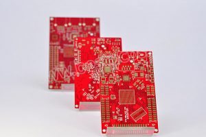
As one of any PCB layer HDI manufacturers in China, EBest Circuit (Best Technology) provides high quality HDI PCB electronics manufacturing and PCBA service. Here are some of our HDI printed circuit boards’ parameters and pictures for your reference.
6 Layers HDI (1+4+1) 4G Module PCB Parameters
- HDI (1+4+1)
- 4G module PCB
- 6 layers FR4 PCBDrill depth control (0.8mm: L1-L3, L6-L3)
- Minmum line width/space: 4/4mil
- 0.1mm Via
- ENIG
- Green Oil

6 Layers HDI (1+4+1) Half Hole Plated PCB Parameters
- HDI (1+4+1)
- Half plated hole
- 0.10mm Buried & Blind Via
- 0.15mm trace width & space
- Multi-layer FR4 PCB
- ENIG
- Green Oil
- White silkscreen

All in all, choosing the right HDI PCB manufacturer is critical for modern electronics projects. EBest Circuit (Best Technology) combines robust HDI PCB fabrication processes, global sourcing, and comprehensive design support to eliminate common customer challenges. Our commitment to precise manufacturing, responsive support, and practical solutions builds trust and drives successful project outcomes for our customers worldwide. If you are finding China leading HDI PCB manufacturer for electronics industry, just contact EBest Circuit (Best Technology) at sales@bestpcbs.com. We are always here to give you practical solutions.
You may also like


Tags: HDI PCB, HDI PCB Fabrication Process, HDI PCB Manufacturer, high density interconnect