

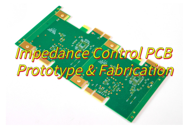
Why choose impedance control PCB? This guide covers specifications, routing techniques, prototyping, and manufacturer selection for reliable high-speed designs.
- Why do your high-speed designs fail EMI tests?
- Is inconsistent impedance ruining your prototype timelines?
- Tired of paying for PCB re-spins due to mismatched impedance?
EBest Circuit (Best Technology) Can Provide:
- Precision Stackup Design: Custom dielectric planning to hit impedance targets (±5%) on the first try.
- Routing Rule Automation: Generate CAD rules for trace width/spacing, eliminating manual errors.
- Test-Coupon Validation: Prototypes include measured impedance reports, so you sign off with confidence.
Welcome to contact us if you have any inquiry for impedance control PCB: sales@bestpcbs.com.
What Is Impedance Control PCB?
An impedance control PCB is a specially designed circuit board where the electrical impedance of signal traces is carefully managed to match desired values (typically 50Ω/75Ω/100Ω). This is achieved through precise calculations of trace width, spacing, dielectric material thickness, and copper weight during manufacturing. Such PCBs are essential for high-frequency digital signals (like DDR memory) and RF/microwave circuits, where mismatched impedance causes signal reflections and data corruption. The control process involves using advanced fabrication techniques and often requires TDR (Time Domain Reflectometry) testing to verify impedance accuracy within ±10% tolerance or better.
How Is Impedance Control Done in PCB?
Here’s a clear breakdown of how impedance control is implemented in PCB manufacturing, presented in actionable steps:
Design Phase Calculations
- Use field solver software to determine trace geometry (width/space) based on target impedance (e.g., 50Ω, 100Ω differential).
- Account for dielectric constant (Dk), copper thickness, and layer stackup.
Material Selection
- Choose laminates/prepregs with stable Dk values across frequencies (e.g., FR-4 for <6GHz, high-frequency materials for RF).
Stackup Configuration
- Define precise dielectric thicknesses between layers to achieve desired impedance.
- Include ground planes adjacent to signal layers for stripline designs.
Fabrication Controls
- Laser Direct Imaging (LDI) ensures trace width accuracy (±0.2 mil).
- Etch compensation adjusts for copper undercut during processing.
Testing & Validation
- Test coupons with identical trace geometry are fabricated alongside PCBs.
- Time-Domain Reflectometry (TDR) verifies impedance values per IPC-TM-650.
Documentation
- Provide impedance reports showing measured vs target values, typically within ±7% tolerance.
PCB Impedance Control Specification
| Target Impedance Values | Specification | Verification Method |
| Target Impedance Values | 50Ω (single-ended), 100Ω (differential) ±10% tolerance | TDR testing across coupon samples |
| Trace Width Tolerance | ±0.2 mil from designed width | Optical measurement system |
| Dielectric Thickness | ±10% of specified value between signal and reference planes | Cross-section microscopy |
| Material Requirements | FR-4 (εr=4.2-4.8) for ≤1GHz; PTFE (εr=2.2-3.5) for RF/microwave | Material certification docs |
| Copper Roughness | ≤1.8µm RMS for high-speed signals (>5Gbps) | Surface profilometer |
| Differential Pair Skew | <5ps/inch length mismatch | TDR/TDT measurements |
| Impedance Test Coverage | Minimum 3 test coupons per panel including edge/center locations | TDR scan documentation |
| Layer Registration | ±1 mil layer-to-layer alignment | X-ray inspection |
| Surface Finish Impact | ≤2% impedance variation from finish (ENIG/Immersion Silver/OSP) | Pre/post-finish TDR comparison |
| Environmental Stability | ±5% impedance shift after 3x reflow cycles (260°C peak) | Thermal stress + retest |
Guide to Impedance Control During PCB Routing
1. Align Trace Dimensions with Stackup
- Use microstrip/stripline calculators (e.g., Saturn PCB Toolkit) to determine trace width/spacing based on dielectric thickness and material Dk.
- Example: For 50Ω single-ended traces on 4-layer FR4 (Dk=4.2), set width to 0.2mm with 0.15mm spacing to adjacent ground.
2. Route Near Solid Reference Planes
- Place high-speed traces directly above/below unbroken ground or power layers to stabilize return current paths.
- Avoid routing across split planes or gaps, which cause impedance fluctuations.
3. Optimize Trace Bends
- Replace 90° corners with 45° miters or arc-shaped bends to reduce signal reflections.
- Use radius ≥3× trace width for curved routing in RF/microwave designs.
4. Space Differential Pairs Precisely
- Maintain fixed intra-pair spacing (e.g., 2× trace width for USB 2.0, 3× for USB 3.0).
- Example: For 0.15mm-wide USB 3.0 traces, set spacing to 0.45mm to ensure consistent coupling.
5. Minimize Vias in Critical Paths
- Use blind/buried microvias (≤0.15mm diameter) for high-speed signals instead of through-hole vias.
- Avoid via stubs by backdrilling or using via-in-pad designs.
6. Isolate Noise-Sensitive Routes
- Keep high-speed traces ≥3× trace width away from switching regulators, crystal oscillators, or power planes.
- Use guard traces (grounded copper pours) between analog/digital domains.
7. Designate Controlled Impedance Layers
- Assign inner layers (e.g., L2–L5) for high-speed routing with predefined stackup parameters.
- Example: L2–L3 for DDR4 traces, L4–L5 for PCIe differential pairs.
8. Collaborate with Fabricators Proactively
- Share routing guidelines (trace tolerance ±10%, via specs) to align manufacturing processes with impedance targets.
- Request impedance coupons for post-fabrication TDR validation.
9. Validate with Post-Route Simulation
- Run SPICE or 3D EM simulations (e.g., Ansys HFSS) to check impedance consistency and signal integrity.
- Adjust trace geometries if simulations show reflections >5% of signal amplitude.
10. Document Manufacturing Constraints
- Include impedance specs, tolerance thresholds, and test methods in fabrication drawings.
- Example: “All 100Ω differential pairs must meet ±8% impedance tolerance, validated via TDR.
How to Add Control Impedance PCB Fabrication Notes?
1. Specify Target Impedance Values
- Clearly state required impedance (e.g., “50Ω single-ended,” “100Ω differential”) for each controlled trace group.
- Include tolerance (typically ±10% for standard designs).
2. Define Stackup Requirements
- List dielectric thickness (e.g., “Prepreg: 0.1mm ±5%”) and copper weight for each layer.
- Note reference plane requirements (e.g., “Adjacent ground planes for striplines”).
3. Trace Geometry Details
- Provide exact width/spacing for impedance-critical traces (e.g., “Differential pairs: 0.15mm width, 0.2mm spacing”).
- Highlight prohibited modifications (e.g., “Do not adjust trace widths without recalculating impedance”).
4. Material Properties
- Specify dielectric constant (Dk) and loss tangent (Df) values used in calculations (e.g., “FR-4, εr=4.3 @1GHz”).
- If using specialty materials, include material grade or manufacturer’s datasheet reference.
5.Validation Method
- Request impedance test coupons matching production parameters.
- Define acceptance criteria (e.g., “TDR-measured impedance within ±8% of target”).
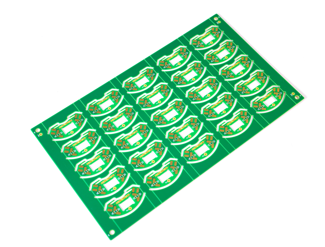
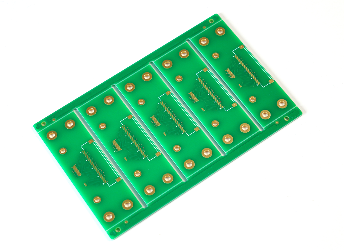
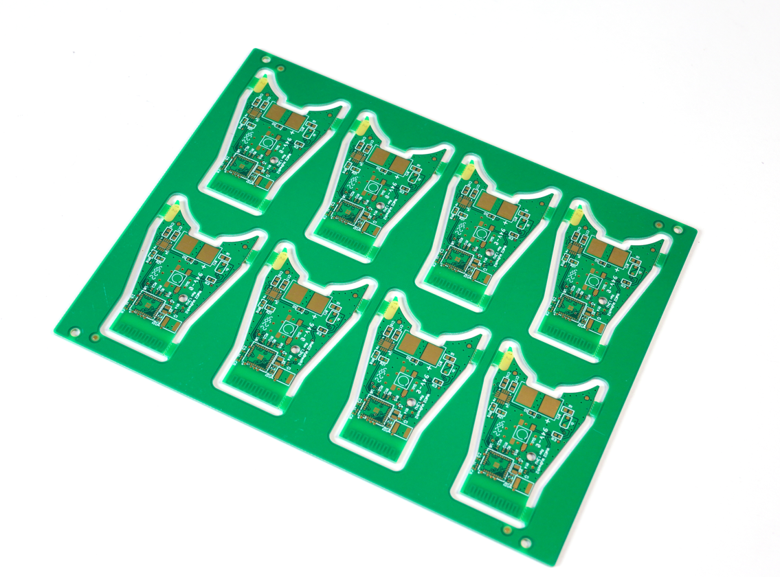
Impedance Control PCB Prototyping Processes
Impedance control PCB prototyping processes
1. Simulate and Adjust Geometry
- Use EM tools (e.g., SIwave) to model traces and refine width/spacing for target impedance (e.g., 50Ω single-ended).
2. Select Materials and Define Stackup
- Choose substrates (e.g., FR4) with stable Dk and loss tangents. Specify core/prepreg thicknesses (e.g., 0.2mm FR4 core for 4-layer boards).
3. Set Manufacturing Parameters
- Collaborate with fabricators on etching tolerances (±10% trace width) and copper thickness (e.g., 1oz/35µm). Specify via drilling/backdrilling depths.
4. Route Traces on Controlled Layers
- Place high-speed signals on layers adjacent to ground/power planes (e.g., Layer 2 signals, Layer 3 ground). Use 45° bends to avoid reflections.
5. Verify In-Process Quality
- Request dielectric/copper measurements during lamination. Use optical tools to confirm trace dimensions.
6. Test Impedance Post-Fabrication
- Validate via TDR on integrated coupons. Compare results to targets (e.g., 100Ω differential pairs ±8%).
7. Analyze Signal Integrity
- Use oscilloscopes/network analyzers to check for reflections or crosstalk. Add termination if needed.
8. Document and Iterate
- Record test data and share feedback with fabricators to refine future builds (e.g., adjust etching time for tighter tolerances).
Impedance Control PCB Manufacturer – EBest Circuit (Best Technology)
Reasons why choose EBest Circuit (Best Technology) as impedance control manufacturer:
Free Impedance Calculation Service: Our engineering team provides complimentary impedance simulations using advanced tools (e.g., SI9000, Polar) to optimize trace width, spacing, and stackup for your design.
Rapid Turnaround Time: 24-hour quick-turn prototyping with guaranteed impedance consistency, ideal for urgent R&D iterations.
Strict Quality Control: IPC-6012 Class 3 standards compliance, 100% TDR testing on impedance coupons, and AOI/4-wire Kelvin testing for trace integrity.
Cost-Effective Pricing: Transparent quotes without hidden fees, leveraging economies of scale and lean manufacturing.
Comprehensive Material Options: Support for FR-4, Rogers, Taconic, and other high-frequency laminates with stable Dk values (1GHz–40GHz).
One-Stop Solution: End-to-end support from design review to volume production, including DFM analysis and impedance reports.
Welcome to contact us if you have any request for impedance control PCB: sales@bestpcbs.com.
You may also like


Tags: impedance control pcb, Impedance Control PCB Prototype