Set the cutoff of a substrate integrated waveguide below your lowest operating frequency, then verify that the feed can launch the desired mode across the whole band. A guide that starts propagating at 7.8 GHz is not automatically usable just above 7.8 GHz. For an X-band design, build a plain guide with two transitions before testing the filter or antenna that uses it. That reference tells you whether a narrow usable band comes from the guide, the launches, or the device itself.
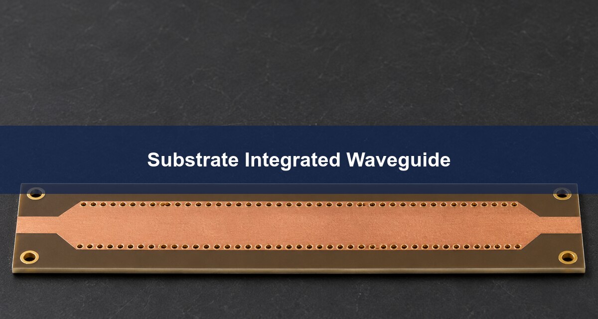
Substrate Integrated Waveguide (SIW): What the Via Rows Do
An SIW traps the field between copper planes above and below the laminate and between two rows of grounded, plated holes. Those holes approximate the solid sidewalls of a dielectric-filled rectangular waveguide. The dominant TE10-like mode has one electric-field maximum across the guide width. If you change the row spacing, you change the condition that allows this field pattern to propagate. The Deslandes and Wu propagation study explains why the periodic wall, rather than just the distance between it and the trace, matters.
| Structure | Choose it when | Main trade-off |
| Conventional microstrip | You need compact planar routing or easy component access. | The field extends outside the laminate; nearby objects and ground geometry matter. |
| Dielectric-filled SIW | You want a confined planar path, cavity filter or slot feed above a defined cutoff. | The laminate and repeated holes affect loss; transitions and lateral area need a budget. |
| Air-filled metal waveguide | Low loss and high power justify a separate mechanical assembly. | Flanges, alignment and enclosure volume add integration work. |
Substrate Integrated Waveguide Design: Start With Four Dimensions
Define row spacing, pitch, via diameter and laminate thickness before drawing the feed. The transverse center-to-center row spacing a largely sets cutoff; the pitch p along each row and modeled via diameter d influence leakage and effective width. The thickness h affects the launch and conductor loss and belongs in the full-wave model, even though it is absent from the simple TE10 cutoff equation.
For a fabricated board, state what your via dimension represents and ask how it maps to drill diameter, finished bore and plated barrel geometry. Model the geometry actually being built instead of changing the drill note and leaving the simulation untouched. Record the laminate construction, design permittivity in the operating band, loss tangent, copper thickness and profile. A nominal Dk from another process or frequency is not a substitute.
SIW Cutoff Frequency: Work Backward From the Band Edge
For an illustrative 10–12 GHz guide with assumed relative permittivity 3.50, a target dominant-mode cutoff of 7.8 GHz gives an effective width of about 10.27 mm. The starting relations are fc ≈ c/(2aeff√εr) and aeff ≈ a − d²/(0.95p). Use meters with c in m/s for frequency; the width correction works with any consistent length unit. These relations appear in the published comparison of equivalent-width models.
With a modeled via diameter of 0.45 mm and 0.70 mm pitch, the width correction is about 0.305 mm. Set the initial row spacing near 10.58 mm, not 10.27 mm. This is a starting layout, not a board specification. Sweep the fabrication tolerances and material permittivity in a full-wave model. Do not tune directly at cutoff: propagation is dispersive there, the required match changes quickly, and a small shift can consume the band-edge margin.
Via Fence PCB Geometry: Check the Sidewall Before the Launch
Tighter spacing generally makes the via wall less leaky, but spacing also has to leave the fabricator enough material between neighboring holes. The example gives d/p ≈ 0.64 and an idealized hole-to-hole gap of 0.25 mm before tolerances. Use that gap to start the DFM conversation, not as the minimum allowable web. Confirm the relevant drill geometry, plating continuity, annular rings and registration. Inspect both fences and the plane connections; a single missing or poorly plated via near a transition can break the symmetry you modeled.
Waveguide Higher Order Mode: Set the Upper Limit Too
The upper edge is not simply the highest frequency at which S21 looks good. In the equivalent thin rectangular guide, the TE20 cutoff is approximately twice the TE10 cutoff, or 15.6 GHz in the example. A symmetric launch can reduce coupling to that mode, but a bend, offset or connector asymmetry can excite modes that a symmetric simulation misses. Check the actual structure for higher-mode excitation and periodic-wall effects above the intended passband rather than assuming operation up to 15.6 GHz.
Microstrip to SIW Transition: Match the Mode as Well as the Feed
A 50-ohm microstrip is only the input. A taper reshapes its field to couple into the SIW mode; its width, length and position must be tuned with the guide and laminate modeled together. See the Deslandes transition design paper and the microstrip PCB guide for their distinct parts of the problem. Start with a back-to-back pair on a short straight guide. Compare it with a second board that uses the same launches and a longer guide.
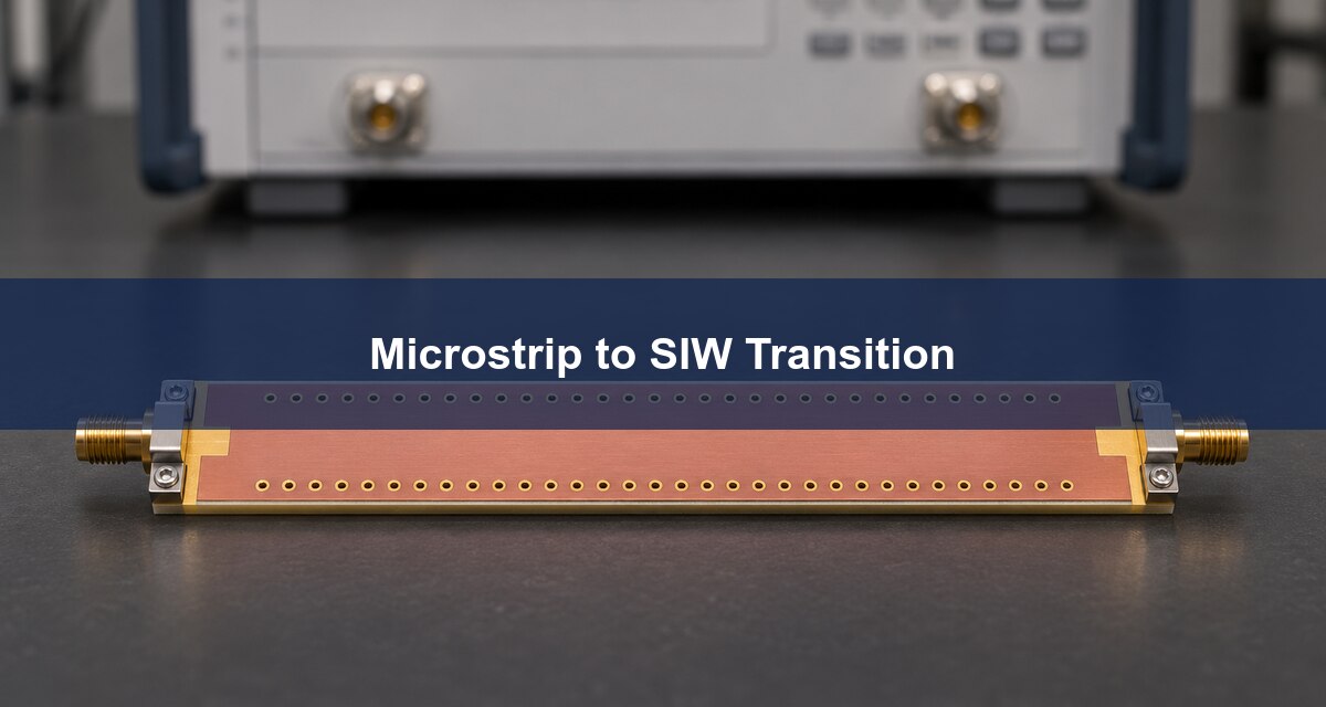
Substrate Integrated Waveguide Filter: Test the Bare Guide First
Do not use the complete filter as the first proof that the feed works. Inductive windows or cavities change coupling and can add passband ripple. First check the transition-only coupon; then add the filter and compare its passband, stopband and return loss. If the plain guide shows the same edge roll-off as the filter, revisit the line and feeds before changing the resonators. For antenna feeds, use the same logic: keep an un-slotted reference to distinguish unwanted line loss from deliberate radiation through a slot.
Waveguide Insertion Loss: Read Two Lengths Before Blaming the Laminate
A single S21 trace combines guide loss, mismatch and launches. When reflections are low and the two boards share the same launch geometry, the additional loss of the longer coupon divided by the additional length estimates distributed attenuation. For a hypothetical 20 mm and 60 mm pair measured at 11 GHz, 1.2 dB and 2.0 dB of positive insertion loss give (2.0 − 1.2)/40 = 0.020 dB/mm. It is not a measurement of laminate Df. If the traces have strong ripple, characterize or de-embed the launches instead of subtracting them as fixed losses.
| Observed result | Check next | Decision |
| Both coupons roll off near the low edge. | Mode cutoff and low-edge reflection. | Increase cutoff margin or retune the launches based on the evidence. |
| Extra loss increases with length and the match stays good. | Dielectric, copper profile and sidewall leakage. | Investigate the guide before changing the feed. |
| Ripple changes sharply after reconnecting. | Connector seating, calibration and calibration plane. | Fix repeatability before judging the PCB. |
Define limits for insertion loss, reflection and unwanted response, plus the frequency band and reference planes, before ordering the coupon. IPC-TM-650 2.5.5.12A is a reference for printed-board loss measurement methods, not an SIW geometry standard or a universal pass limit.
FAQ
Can a ground via fence beside a trace act as an SIW?
Not by itself. A standard SIW needs two conducting planes and two sidewall rows enclosing a dielectric-filled path, with a launch that excites its guided mode.
Can I use FR-4 for an SIW prototype?
It can be useful to test topology. Use the actual laminate’s frequency-dependent properties and measure the application band before treating the prototype as a low-loss production design.
Is SIW cutoff the same as the filter’s lower passband edge?
No. The guide cutoff governs propagation; the filter edge also depends on its resonators, coupling and transitions. Test the bare guide separately.
Why not shrink the guide with a higher Dk laminate?
A higher Dk can shrink the guide for the same cutoff. Recalculate the via geometry and matching, then check loss and tolerance sensitivity rather than scaling only the width.
Should I model the solder mask?
Include it where it affects exposed microstrip or transitions, and keep the prototype and model consistent. Do not use a coating correction intended for the feed as a bulk SIW correction.
Can I validate the design with only a 50-ohm impedance coupon?
No. That coupon can check the feed’s impedance, but it does not verify mode conversion, loss or the SIW operating band.
Do the two guide coupons need equal connector types?
Yes, and match installation, feed dimensions and calibration. The length difference should be intentional; differences in connector placement or soldering undermine the comparison.
What should I send for a fabrication review?
Send the target band, stackup, modeled via geometry, actual drill and plating requirements, the two row dimensions and the drawing for each test coupon.
Prepare the SIW Stackup and Coupon Package
For a Best Technology fabrication discussion, email sales@bestpcbs.com with the stackup, allowed drill and layer shifts, and the frequency limits that the two coupons must verify. Identify which dimensions can move and which are fixed by your RF model.
You may also like




Tags: Microstrip Transition, RF PCB, Substrate Integrated Waveguide, Waveguide Cutoff