





This specialized semiconductor packaging and testing companies list includes ASE Technology Holding, Amkor, JCET, Powertech, Tongfu, Huatian, ChipMOS, Hana Micron and UTAC. These providers operate in semiconductor back-end manufacturing: connecting and protecting dies, then testing devices against electrical requirements. Their portfolios differ across memory, logic, RF, power and multi-die integration. Choosing a provider starts with the device, package and test flow—not a company’s name alone.
At EBest Circuit, we work at the downstream PCB and PCBA stage. We help customers manufacture circuit boards and assemble packaged components; we are not presenting ourselves as an OSAT provider. Understanding the package handoff helps our customers prepare the footprint, assembly process and board-level tests correctly.
Key Takeaways
- OSAT means outsourced semiconductor assembly and test; the assembly is primarily at die and package level.
- The list covers nine providers with publicly documented packaging and test services, not a revenue ranking or an endorsement.
- ASE and SPIL belong under ASE Technology Holding; counting them separately can duplicate a corporate group.
- Memory, display-driver, power, RF and advanced multi-die products require different package and test capabilities.
- Wafer probe, final test, burn-in and system-level test serve different purposes; confirm the required flow and site.
- Semiconductor package qualification does not replace PCB assembly inspection or finished-board functional testing.
Which Companies Offer Packaging and Test?
ASE Technology Holding, Amkor, JCET, Powertech, Tongfu, Huatian, ChipMOS, Hana Micron and UTAC provide packaging and test services with different technology and application emphases. The following list of semiconductor packaging companies summarizes those distinctions.
| Provider | Publicly described service focus |
| ASE Technology Holding, including ASE and SPIL | Broad package assembly, testing and heterogeneous integration |
| Amkor Technology | Package development, wafer bumping, assembly and multiple test stages |
| JCET Group | Package design, integration, assembly and testing |
| Powertech Technology (PTI) | Memory and logic probing, packaging, final test and module services |
| Tongfu Microelectronics | Packaging and test for computing, communications, automotive and other devices |
| Huatian Technology | Leadframe, memory, SiP, wafer-level and fan-out services |
| ChipMOS Technologies | Display-driver, memory and mixed-signal back-end services |
| Hana Micron | Bumping, wafer test, assembly, final test and modules |
| UTAC Group | Leadframe, laminate, wafer-level, SiP, power and test services |
Scope checked against public company materials on October 29, 2026. Inclusion does not establish that every plant supports every package, that capacity is available, or that a supplier accepts a particular prototype quantity.
What Does Each Provider Focus On?
The useful differences are each provider’s package portfolio, device experience and test coverage. The summaries below explain where to begin a technical discussion without treating the suppliers as interchangeable.
ASE Technology Holding
ASE Technology Holding brings together ASE, SPIL and USI. ASE’s semiconductor services include package design, assembly and test, while its heterogeneous-integration work addresses combinations of dies and components in a package. SPIL is part of the same holding group, not a separate independent group entry in this list.
For sourcing, identify the operating company and qualified site behind the proposal. A group-level technology presentation is not a site-specific production approval.
Amkor Technology
Amkor offers package design support, characterization, wafer bumping, assembly and test. Its published test portfolio includes wafer probe, final test, burn-in and system-level test, with applications covering compute, communications, automotive, memory and other device types.
Its breadth makes the test strategy part of the package discussion. Define whether the project needs wafer-level screening, post-package electrical coverage, operating-temperature testing or a system-level insertion.
JCET Group
JCET describes an integrated service chain covering packaging design, system integration and testing. It is a provider to evaluate when package development and assembly/test execution need to be coordinated rather than purchased as unrelated steps.
For a multi-die project, request the proposed interconnect architecture, thermal model and package-to-board interface. Do not assume that an advanced-platform name identifies one fixed structure or a universally available production line.
Powertech Technology
Powertech, commonly abbreviated PTI, publishes services for chip probing, wafer-level packaging, flip-chip packages, wire-bond BGA, SiP and module assembly. Its final-test coverage explicitly includes DRAM, NOR flash, NAND flash, multi-chip packages and logic devices.
Memory projects should match the provider’s test platform to the actual device generation and organization. Package compatibility alone does not prove test-program readiness or the required parallel-test throughput.
Tongfu Microelectronics
Tongfu publishes services from design simulation and wafer testing through packaging, final test and system-level test. Its stated application coverage includes computing, communications, automotive, memory and other semiconductor categories.
For a compute device, discuss package routing, power delivery, thermal control during test and the required test stages together. A high-power device may need specialized handling and temperature management beyond a standard final-test setup.
Huatian Technology
Huatian’s public portfolio includes SiP, memory, MEMS and wafer-level fan-out packaging. Its test services cover program development, wafer probing, final test and system-level test.
This range spans very different manufacturing flows. Confirm whether the proposal is for a leadframe package, substrate-based package or wafer-level architecture, and which site will perform the work.
ChipMOS Technologies
ChipMOS focuses on back-end services for display-driver ICs, memory and mixed-signal devices. Its published assembly portfolio includes leadframe and organic-substrate packages, with bumping and display-related interconnect services.
A display-driver project should specify whether its interface is chip-on-film, chip-on-glass or another format. Those interfaces are not interchangeable with an ordinary board-mounted BGA or QFN.
Hana Micron
Hana Micron describes a turnkey service chain including bumping, wafer probe, assembly, final test and modules. Its materials discuss a memory-packaging base and expansion into non-memory packaging and test.
Match the inquiry to a documented package family and test requirement. Do not turn a development roadmap into an assumption that a particular advanced package is already qualified for the intended product.
UTAC Group
UTAC publishes leadframe, laminate, SiP, wafer-level, MEMS/sensor and power-package services, alongside wafer sort, final test, test development and reliability services.
For analog, mixed-signal, sensor or power products, define the electrical stimulus, measurement limits and thermal conditions early. Specialized semiconductor testing and packaging companies need device-specific coverage, not simply a request to “test all chips.”
What Is an OSAT Company?
An OSAT company is an outsourced semiconductor assembly and test provider that turns semiconductor dies into tested packages or performs selected stages of that back-end flow. Customers may be fabless chip companies, integrated device manufacturers or other semiconductor businesses.
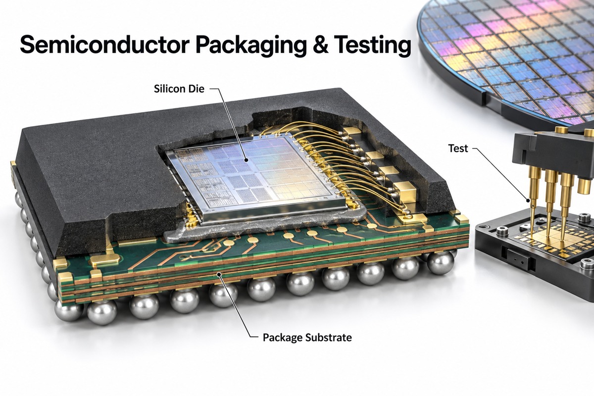
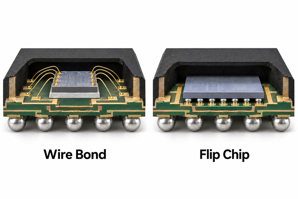
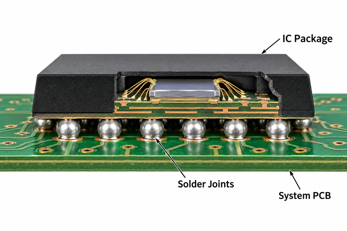
Semiconductor chip packaging companies connect die pads to the package’s external terminals and protect the die mechanically. Depending on the architecture, the connection can use bond wires, flip-chip bumps, redistribution layers, interposers or combinations of these structures.
For a closer explanation of package construction, see our IC packaging guide. Packaging is not the same operation as fabricating the transistors on a wafer, although wafer-level packaging can involve processes performed on a wafer before singulation.
Which Semiconductor Test Services Are Different?
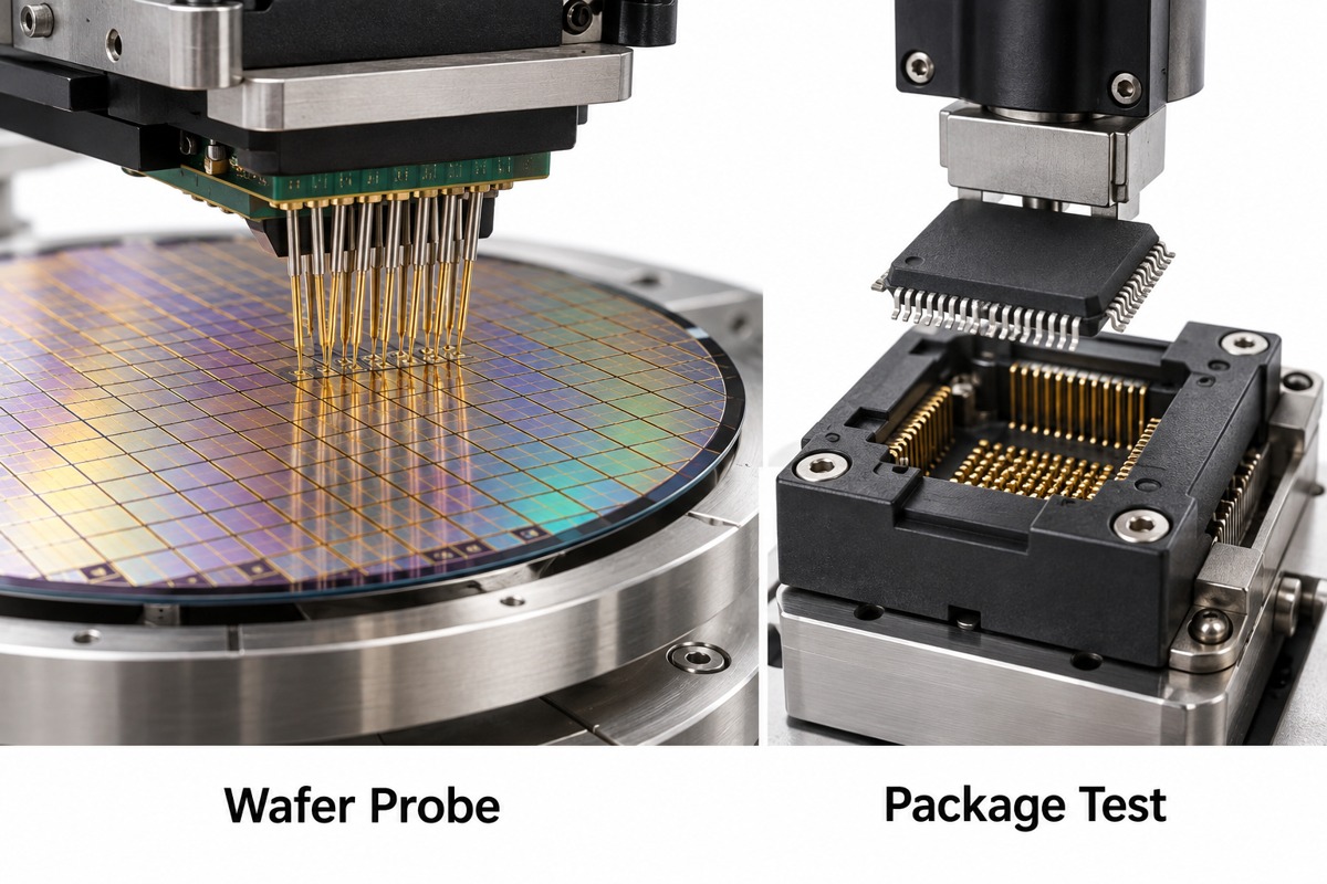
Wafer probe checks dies before packaging, final test checks packaged devices, burn-in applies a specified stress screen, and system-level test exercises devices in a more application-like environment. They are complementary stages, not different names for the same inspection.
| Test stage | Test object | Main purpose |
| Wafer probe or wafer sort | Dies on a wafer | Electrical screening and binning before assembly |
| Final test | Packaged device | Verify specified electrical and functional limits |
| Burn-in | Wafer or packaged devices, depending on flow | Apply defined voltage/temperature stress screening |
| System-level test | Device in a test system | Exercise application-like workloads or interactions |
| Reliability qualification | Specified samples and structures | Evaluate a defined qualification plan |
“100% tested” needs a definition: which units, which parameters, at what temperature, with which guardbands and test limits? It does not mean every possible failure mechanism has been eliminated. Qualification sampling also differs from production screening.
How Do Advanced Packaging Providers Differ?
Compare advanced semiconductor packaging companies against the actual package architecture, interconnect requirements, thermal load and qualification status—not the word “advanced” in a brochure.
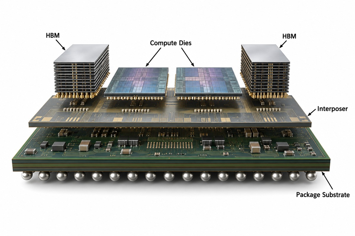
- Architecture: wire bond, flip chip, fan-out, SiP, 2.5D or 3D integration.
- Physical interface: die dimensions, die-to-die connections, external ball map and package outline.
- Electrical behavior: power distribution, signal bandwidth and parasitic models.
- Thermal and mechanical behavior: cooling interface, warpage, materials and stress.
- Production evidence: qualified site, process maturity, test coverage and change-control responsibilities.
For example, a multi-die logic-and-HBM package needs short, dense package-level connections and coordinated power and thermal design. A small power package may instead prioritize its current path, heat flow and isolation requirements. The same supplier can address both through different technology platforms and production flows.
What Should You Confirm Before Choosing an OSAT?
Confirm the package, qualified manufacturing site, test ownership, capacity arrangement and commercial scope before selecting a provider. A public service portfolio is a starting point, not an accepted manufacturing commitment.
- Define the incoming material: wafer, singulated die, known-good die or partly processed assembly.
- Agree on the package drawing, materials and interconnect architecture.
- Assign responsibility for test development, sockets, load boards and correlation.
- Document qualification, traceability, failure-analysis access and change notification.
- Separate development tooling and non-recurring engineering from recurring production charges.
- Confirm available capacity, minimum order terms and the transition from engineering lots to production.
Choose the technical flow first, then compare like-for-like quotations. The lowest unit assembly price may exclude test development, substrate tooling or another required step.
How Is OSAT Different from PCB Assembly?
OSAT primarily connects bare semiconductor dies into packages; PCB assembly solders packaged components and other parts onto a circuit board. The two stages have different inputs, equipment and acceptance tests.
| Item | Semiconductor packaging and test | PCB assembly |
| Typical input | Wafer or bare dies | Bare PCB and electronic components |
| Interconnect | Bond wires, microbumps or package routing | Solder joints, connectors and board traces |
| Typical output | Tested IC package or module | Populated circuit board |
| Acceptance focus | Package integrity and device specifications | Assembly quality and board functions |
At the handoff, the board designer needs the exact package drawing, recommended land pattern, moisture-sensitivity handling and allowed assembly profile. Internal die-to-die bump pitch must never be used as the PCB’s external pad pitch.
Our PCB assembly services address that board-level stage. Device test results do not replace inspection of the solder joints or verification of power, firmware and interfaces on the finished board.
FAQ About Semiconductor Packaging and Testing Companies
Are foundries and OSAT providers the same?
No. Foundries primarily manufacture semiconductor wafers, while OSATs specialize in outsourced assembly and test. Some foundries also offer advanced packaging, so compare the specific service rather than assume one company type has only one capability.
Should ASE and SPIL be counted separately?
They can be discussed as operating businesses, but both are within ASE Technology Holding. This list treats the holding group as one entry to avoid presenting two group businesses as independent corporate alternatives.
Can a small hardware company order a few packaged custom chips?
Acceptance depends on the provider, technology and project terms. Engineering support, tooling and test-program development may dominate a small lot’s cost. Confirm the minimum engagement and development scope directly instead of assuming prototype-PCB ordering terms apply.
Does every OSAT provide leading-edge 2.5D packaging?
No. A provider may specialize in leadframe packages, memory, display drivers or other products. Even when advanced packaging is advertised, verify the particular architecture, site and qualification status for your device.
Do packaging providers make the package substrate themselves?
Not necessarily. The substrate can come from a specialist supplier and be integrated by the package assembler. Clarify who owns substrate design, supplier qualification, procurement and incoming inspection.
Does passing chip final test guarantee a working PCBA?
No. Board-level faults can still arise from soldering, power delivery, incorrect parts, firmware or interface design. A working assembly requires its own inspection and functional acceptance plan.
How Can EBest Circuit Support Your PCBA?
We support PCB fabrication, component sourcing and PCBA after the semiconductor package interface is defined. Our review connects the package land pattern to board construction, assembly access and the agreed functional tests.
If you are integrating packaged ICs into a new product, contact sales@bestpcbs.com. We can review the board-manufacturing and assembly scope, while the semiconductor packaging provider remains responsible for its die-level process and package qualification.
You may also like


Tags: advanced semiconductor packaging companies, list of semiconductor packaging companies, semiconductor chip packaging companies, semiconductor testing and packaging companies, specialized semiconductor packaging and testing companies list