An ATE load board connects automatic test equipment to the device under test (DUT), carrying the signals and power used to measure an IC’s performance. Because it sits directly in the measurement path, its routing, power connections, and socket contacts can affect the result. A chip that appears to fail may instead be receiving a distorted signal, an unstable supply, or an unreliable connection.
EBest Circuit (Best Technology) supports PCB fabrication, component sourcing, and PCBA assembly from customer-provided designs. Our manufacturing review addresses details such as plated-hole construction, board thickness, and socket mounting before fabrication and assembly. For your load board PCB or PCBA project, contact sales@bestpcbs.com.
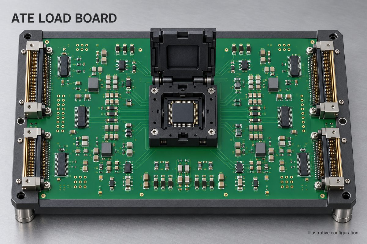
What Is an ATE Load Board?
An ATE load board is the electrical interface between a semiconductor tester and the chip being tested. It maps tester resources to the DUT pins and provides the local circuitry required by the test application.
For a typical packaged-device test, the connection follows this path.
Tester → tester interface → load board → test socket or contactor → DUT
The tester supplies stimuli and measures responses. The load board routes those connections; the socket makes temporary contact with the device. A handler may position and press the packaged device into the contactor.
You may also see this hardware described as a device interface board (DIB). The terms overlap, although their exact usage varies between tester platforms.
What Components Are on an ATE Load Board?
Tester contacts and a DUT socket form the two ends of the connection. Between them, the board may contain switching circuits, local power components, and signal-conditioning networks.
- Tester connectors or contact pads bring individual tester channels onto the PCB. Board traces then connect those channels to the assigned DUT pins.
- The socket or contactor touches the package leads, lands, or solder balls. It allows devices to be exchanged without soldering each chip onto the board.
- Relays or electronic switches can connect a DUT pin to different instruments during different test steps, such as switching between a voltage source and a measurement path.
- Decoupling capacitors provide current close to the DUT when its demand changes quickly. Their placement affects the length of the current loop.
- Passive networks perform specific circuit functions—for example, a termination resistor can reduce reflections, while a sense resistor can produce a voltage proportional to current.
- A stiffener supports the PCB against bending during docking or device contact. Its openings also need to accommodate the socket and surrounding components.
The circuit determines which of these parts are needed. Adding a relay, for example, also adds contacts and parasitic capacitance to the signal path, so switching flexibility comes with electrical trade-offs.
How Does a Load Board Differ from a Probe Card or Burn-in Board?
The main difference is the test task and how the device is contacted. These boards belong to related test environments, but they are not interchangeable.
| Hardware | Typical connection | Main purpose |
|---|---|---|
| Load board for packaged-device ATE | Tester to packaged IC through a socket or contactor | Route signals and power for electrical measurements and functional tests |
| Probe card | Tester interface to pads or bumps on a wafer through probes | Establish contact for testing devices before singulation |
| Burn-in board | Burn-in system to devices held in sockets or other contacts | Connect devices during sustained, specified electrical and thermal stress |
A wafer-test setup can also include an interface board between the tester and probe card.
Temperature alone does not separate load boards from burn-in boards. Packaged-device ATE testing can also take place at hot or cold temperatures. Burn-in differs primarily in its stress-screening purpose and test duration.
How Does ATE Load Board Design Affect High-Speed Signals?
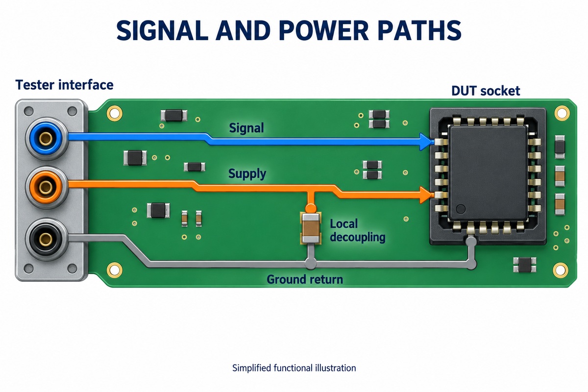
The entire channel affects the waveform reaching the DUT, including traces, vias, connectors, switches, and socket contacts. A controlled-impedance trace cannot compensate for every discontinuity elsewhere in that path.
- Reflections arise at impedance changes and can produce ringing or shift the time at which a signal crosses a threshold.
- Insertion loss reduces signal amplitude along the channel, potentially leaving less margin at the receiver.
- Crosstalk couples energy from nearby channels into the measured signal, making a result depend on neighboring activity.
For example, a trace crossing a gap in its reference plane forces return current to take a longer path. That change can increase noise and disturb the channel impedance. An unused branch or via stub can also reflect part of the signal back toward its source.
Signal edge speed matters even when test patterns repeat slowly. A fast transition still travels through every connector, via, and socket contact in the channel.
How Does the Load Board Deliver Stable Power to the DUT?
The voltage at the DUT depends on the complete supply and return path. Copper, vias, connectors, and contacts all contribute resistance; changing current also interacts with path inductance.
Steady-current voltage drop
For an illustrative total supply-and-return resistance of 0.05 Ω carrying 2 A, the resistive drop is calculated as follows.
V = I × R = 2 A × 0.05 Ω = 0.10 V
That is a 0.10 V difference between the source and load before other effects are considered. Where supported, remote-sense connections allow the supply to regulate voltage at the sensing location, within its compensation limits.
Fast changes in current
When the DUT switches rapidly, local decoupling helps supply the immediate current demand. Short connections between the capacitors, DUT supply, and return reduce the inductance of that loop.
The sense connection measures voltage at its connection point. If that point is upstream of a resistive socket contact, the voltage drop across that contact remains outside the sensed path. Local decoupling addresses faster current changes that the supply’s control loop cannot immediately follow.
What Determines Load Board PCB Materials and Layer Count?
Dense DUT connections can require more routing layers, while longer high-speed channels may call for lower-loss materials. These are separate demands: a board can need many layers for connectivity without every signal requiring an expensive laminate.
Routing out of the socket area
Closely spaced contacts leave limited room for traces and vias. Additional routing layers provide more paths out of that crowded area. Multiple DUT sites add further connections, although the increase depends on which tester resources are shared.
Providing signal returns and power distribution
Some layers are reserved for ground references and power distribution. The spacing between a signal trace and its reference plane affects impedance, so the stackup and trace geometry are developed together.
Controlling loss along longer channels
Signals lose energy as they travel through the board. For a demanding high-speed channel, the material’s dielectric loss, copper characteristics, and route length contribute to the loss budget. A short, slower connection may not need the same material construction.
Manufacturing the holes through the stackup
If a revised stackup increases board thickness while the drilled hole stays the same size, the hole’s aspect ratio increases. Plating that deeper, narrower hole becomes more demanding. Layer additions therefore need to be reviewed alongside hole size, via structure, and the board’s mechanical fit.
How Do Socket Contact and Board Flatness Affect Test Repeatability?
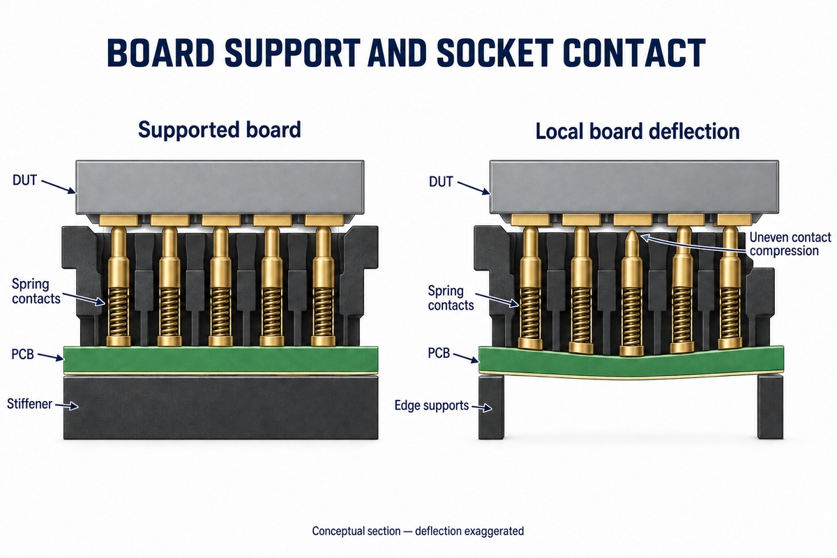
A changing contact can change the measurement even when the DUT has not changed. Contamination, wear, misalignment, or unsuitable contact compression can produce variable resistance or intermittent connections.
In a spring-contact socket, each contact needs enough compression to engage reliably. If the PCB bends locally, some contacts may compress less than others. A poor connection can then appear as an open circuit or add resistance to a power or measurement path.
A stiffener limits board deflection. Socket seating, mounting height, and alignment determine how the contacts meet the device. These mechanical details affect whether repeated insertions reproduce the same electrical connection.
Useful troubleshooting clues
- A result changes after reinserting the same device.
- Failures concentrate at one test site or a recurring group of pins.
- Measured resistance changes with contact engagement.
Repeating the measurement with a reference device while holding the program and temperature constant helps separate contact-related variation from changes in the device or test conditions.
How Is an ATE Load Board Tested Before Production Use?
Testing covers physical connections, powered operation, and measurements on the intended ATE setup. The sequence below describes common checks; the circuit and test application determine which measurements are needed.
1. Check the bare PCB for opens and shorts
Electrical testing compares the fabricated copper connections with the netlist. It detects missing connections and unintended connections between nets. Board dimensions, mounting holes, and socket-area features are inspected against the fabrication drawing.
2. Inspect the assembled board and exercise switching paths
Inspection looks for incorrect components, reversed polarity, solder bridges, and poor joints. Where relays or switches are fitted, commanding each state and measuring the corresponding connection can reveal an open path, a stuck contact, or incorrect routing.
3. Measure power at the DUT connection under load
An unloaded rail reading can look correct even when the path has excessive resistance. Measuring near the DUT while current flows reveals voltage drop. Observing the rail during changes in DUT activity can expose transient dips or ringing.
4. Measure critical signal paths
For channels with demanding timing or bandwidth, time-domain reflectometry can locate impedance discontinuities. Network-analyzer measurements can characterize insertion loss, reflections, and coupling between channels. These measurements require an appropriate fixture and calibration; they are not necessary for every net.
5. Run reference devices and compare results
On the target tester, repeat measurements with characterized reference devices. Compare results with the established reference setup and, where relevant, across test sites. A consistent offset at one site or variation after reinsertion can direct investigation toward that site’s signal, power, or contact path.
Acceptance limits come from the device test specification and the agreed correlation plan. A PCB open/short pass covers connectivity; production release also needs evidence that the assembled board supports the intended measurements.
FAQs About ATE Load Boards
Can one load board work with different ATE platforms?
Load boards are usually built around a particular tester interface. Two platforms may use different channel assignments, power connections, or docking hardware, even if the boards look similar. Moving a design to another platform may require a new interface or board layout.
Can a load board test several chips at once?
Yes. A multi-site board carries several DUT positions. However, several sockets do not mean every measurement runs simultaneously. If sites share one measurement instrument, that part of the test may run sequentially.
Does every new chip require a new load board?
Related devices can sometimes share a board. The same package alone is insufficient: a pin used for power on one device might serve a different function on another. Pin assignments, supply levels, and required test connections determine whether reuse is practical.
Is an evaluation board the same as a load board?
An evaluation board commonly provides bench-accessible connectors and configuration options for development. A production load board connects the device to assigned ATE resources and accommodates the production contact arrangement. Converting between the two can require changes to both routing and mechanics.
When should socket contacts be cleaned or replaced?
Use the contactor supplier’s cleaning method and replacement guidance. Rising contact resistance, visible wear, or recurring contact-related failures can trigger maintenance. Repeated retesting without addressing a worn or contaminated contact can hide the underlying problem.
For your next ATE load board project, EBest Circuit (Best Technology) can support PCB fabrication and assembly from your approved design. Send the PCB files and, for assembly, the BOM and assembly drawing to sales@bestpcbs.com to discuss construction, socket installation, and production options.