

An RF PCB antenna is a conductive trace fabricated directly onto the printed circuit board itself, serving as the essential component for transmitting and receiving electromagnetic waves in wireless devices. This article delves into the fundamentals, design intricacies, and integration challenges of these antennas, exploring how advanced multilayer and HDI PCB designs are pivotal for achieving reliable radiation performance in modern compact electronics.
Are you constantly wrestling with signal integrity issues that appear only after prototyping, or struggling to fit a capable antenna into an ever-shrinking board space? Common pain points include:
- Complex Boards: RF PCB antenna performance becomes unstable in dense multilayer layouts.
- Repeated Redesigns: Trial-and-error RF PCB antenna design causes multiple PCB re-spins.
- Unclear Diagrams: RF PCB antenna diagram files fail to reveal real current flow or radiation behavior.
- Antenna Selection: PCB antenna vs external antenna decisions involve hard-to-balance size, cost, and performance trade-offs.
- Production Drift: RF PCB antenna performance often changes from prototype to mass production.
The solution lies in a holistic approach that bridges expert design with precision manufacturing. By partnering with a PCB manufacturer deeply versed in high-frequency and HDI technologies, you can systematically overcome these hurdles:
- System-Level Co-Design: Antenna performance is co-optimized with multilayer stack-up from the schematic stage using simulation.
- Simulation-Driven Prototyping: Industry-standard RF PCB antenna design software validates performance before fabrication, reducing PCB re-spins.
- Clear Design Transparency: rf pcb antenna diagram intent and RF behavior are clearly documented and explained for system-level understanding.
- Compact HDI Integration: High-performance pcb antenna structures are efficiently embedded in multilayer and HDI boards.
- Production-Level Repeatability: Tight control of materials, etching, and soldermask ensures consistent rf pcb antenna performance from prototype to mass production.
At BEST Technology, we are a specialized manufacturer of high-performance, high-density interconnect (HDI) and multilayer PCBs. We understand that an RF PCB antenna is not an isolated component but a system-critical feature that interacts with every layer of your board. Our core expertise lies in fabricating complex PCBs with the tight tolerances, advanced materials, and controlled impedance required for reliable RF performance. From initial RF PCB antenna design consultation to full turnkey PCBA assembly, we provide the technical partnership needed to bring robust wireless products to market. Pls feel free to contact our team at sales@bestpcbs.com to discuss your project.
What Is an RF PCB Antenna?
An RF PCB antenna is the most integrated form of antenna, where the radiating element is formed from copper traces on the printed circuit board itself. This section introduces its core concept and fundamental value proposition in modern electronics.
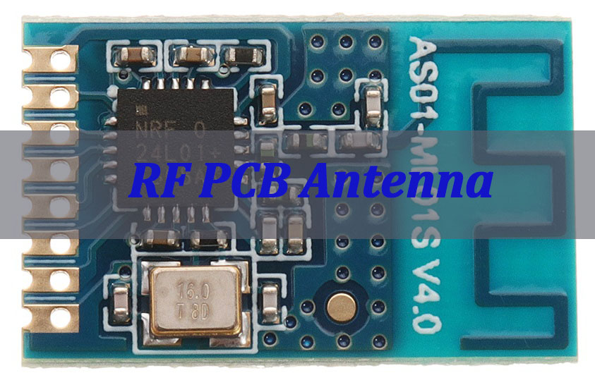
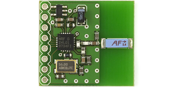
- Definition & Integration: It is a conductive pattern, typically etched on the board’s outer or inner layers, designed to resonate at specific frequencies for wireless communication (e.g., Wi-Fi, Bluetooth, Zigbee, cellular).
- Core Advantages:
- Extremely Low Cost: Eliminates the need for a separate, purchased antenna component.
- Minimal Footprint: Ideal for space-constrained, compact device designs.
- Perfect for Assembly: Streamlines the PCBA process with no additional assembly steps for antenna mounting.
- Design Flexibility: Can be tailored into various shapes (meander, inverted-F, patch) to fit available board space.
While offering significant benefits, its performance is highly sensitive to the PCB’s design and material properties, making expertise in RF PCB antenna design critical.

How Does RF PCB Antenna Work on a Printed Circuit Board?
Its operation is governed by the principles of electromagnetism. When an RF signal is delivered via a transmission line, it excites electrons in the antenna trace, creating an alternating current. This time-varying current generates a corresponding electromagnetic field that radiates into space.
The key to efficient radiation is resonance, where the antenna’s physical length is a specific fraction (e.g., ¼ wavelength) of the target frequency.
The surrounding PCB environment—especially the ground plane size and shape, nearby components, and board dielectric—directly influences the current distribution, impedance, and ultimately, the PCB antenna radiation pattern.
Common PCB Antenna Types Used in Wireless RF Applications
Selecting the right PCB antenna types is the first critical step in design. Each type offers a different balance of size, bandwidth, and performance.
| Antenna Type | Key Characteristics | Typical Applications | Pros & Cons |
|---|---|---|---|
| Inverted-F Antenna (IFA) | Folded monopole, ground-dependent | Bluetooth, WiFi, Zigbee | Pro: Size–performance balance Con: Limited bandwidth |
| Monopole Antenna | λ/4 straight trace | Remote controls, basic RF links | Pro: Simple, omnidirectional Con: Needs vertical space |
| Meandered Monopole | Folded trace, compact layout | Compact consumer devices | Pro: Space-saving Con: Lower efficiency |
| Microstrip Patch Antenna | Planar patch over ground | GPS, directional RF systems | Pro: Low profile, directional Con: Larger area |
| Chip Antenna (SMD) | PCB-mounted RF component | IoT sensors, wearables | Pro: Ultra-small size Con: Layout-sensitive |

Key Principles Behind RF PCB Antenna Design for Stable Radiation Performance
Achieving a reliable RF PCB antenna design requires adherence to several foundational principles, especially within multilayer boards.
- Careful Material Selection: The PCB substrate’s dielectric constant (Dk) and loss tangent (Df) are paramount. A stable Dk ensures predictable resonance, while a low Df (e.g., Rogers materials, high-frequency FR4) minimizes signal loss as heat, directly impacting range and efficiency.
- Controlled Impedance & Matching: The antenna must be matched to the transceiver’s output impedance (typically 50Ω) to maximize power transfer. This involves designing the feedline as a controlled impedance trace and using a matching network (PI or L-circuit) to “tune out” reactances. An rf pcb antenna calculator is a useful starting point, but simulation is essential.
- Ground Plane Management: The ground plane is part of the antenna. Its size, shape, and continuity under the antenna are critical. Improper grounding (e.g., cuts or slots) can severely distort the radiation pattern and detune the antenna.
- Isolation and Keep-Out: A clear keep-out area must be maintained around the antenna. Placing components, especially metal (batteries, shields) or noisy digital circuits, too close will de-tune the antenna and couple noise, degrading performance.
- Simulation-Driven Iteration: Using professional RF PCB antenna design software (like Ansys HFSS, Keysight ADS, or even Simulia CST) is non-negotiable for modern designs. It allows virtual testing of radiation patterns, impedance, and the impact of the enclosure before any board is fabricated.
How to Read an RF PCB Antenna Diagram to Analyze Current Flow and Radiation Pattern?
An RF PCB antenna diagram is more than just a copper shape; it’s a map of electromagnetic behavior. To read it effectively:
- Identify the Feed Point: Locate where the RF signal is injected. This is the highest current density point.
- Trace the Radiating Element: Follow the primary trace from the feed point. Its length and path determine resonance. Bends and meanders increase inductance, effectively making the antenna electrically longer.
- Analyze the Ground Connection: For monopole/IFA types, the ground connection point is crucial. The current return path through the ground plane creates the image of the antenna, completing the dipole structure.
- Visualize Current Flow: Current is maximum at the feed point and (for a λ/4 monopole) zero at the open end. The alternating current along this trace is what creates the radiating field.
- Deduce Radiation Pattern: The antenna’s orientation and the ground plane’s extent dictate the pattern. A vertical monopole over a large ground radiates omnidirectionally in the horizontal plane. The PCB antenna radiation pattern from a simulation overlay on the diagram shows the 3D radiation strength.
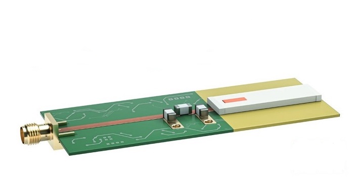
Comparing PCB Antenna vs External Antenna in Compact RF Device Design
The debate between PCB antenna vs external antenna is central to RF product design. The choice hinges on performance, cost, size, and development effort.
| Feature | PCB Antenna | External Antenna |
|---|---|---|
| Cost | Very low | Higher |
| Integration | Fully integrated | Requires mounting |
| Size | Compact, low profile | Needs 3D space |
| Performance | Layout dependent | More consistent |
| Bandwidth | Narrower | Wider |
| Design Effort | High | Low |
| Best Fit | Compact, high-volume devices | Long-range, critical RF links |
For devices using multilayer and HDI PCB designs, the integrated PCB antenna often becomes the only viable option due to space constraints, making expert design and fabrication even more critical.
How Do You Test an RF PCB Antenna After PCB Fabrication?
Post-fabrication testing validates the design and ensures manufacturing consistency. Key tests include:
- Vector Network Analyzer (VNA) Measurement: The primary tool. It measures the S11 parameter (Return Loss), showing how well the antenna is matched at the target frequency (e.g., S11 < -10 dB indicates a good match).
- Impedance Measurement: The VNA plots the antenna’s complex impedance (Z = R + jX) across frequency, allowing for precise matching network adjustments.
- Passive/Active Range Testing: The assembled device is placed in an anechoic chamber to measure its actual pcb antenna radiation pattern, gain, and efficiency—the ultimate performance indicators.
- Conducted Power & Sensitivity: Testing the connected RF transceiver’s output power and receiver sensitivity with the integrated antenna ensures the full radio chain works as intended.
How Can an RF PCB Antenna Be Integrated Into HDI PCBs?
HDI technology, with its micro-vias and finer traces, offers unique advantages for advanced RF PCB antenna integration, enabling more reliable and compact designs.
- 3D Integration & Saved Real Estate: Antenna traces can be routed on different layers and connected with controlled-depth micro-vias, creating complex 3D structures in a small footprint, like an inverted-F antenna that uses vertical vias for the shorting stub.
- Improved Isolation: Sensitive antenna feedlines can be embedded between solid ground layers in the HDI stack-up, shielding them from noise from other board sections.
- Precision and Consistency: HDI processes allow for extremely precise etching of fine antenna traces and via stubs, which is crucial for high-frequency (e.g., mmWave) antennas where tolerances are microscopic.
- Direct Integration with RF Front-End: The antenna can be seamlessly connected to filters, amplifiers, and switches on the same HDI board with ultra-short, low-loss interconnects, minimizing parasitic losses.
How EBest Circuit (Best Technology) Supports RF PCB Antenna Projects From PCB Prototype to PCBA Mass Production?
Our support is a seamless, integrated service that addresses the entire lifecycle of your product.
- Design for Manufacturing (DFM) Consultation: We review your RF PCB antenna design and stack-up early, advising on material selection, stack-up for optimal grounding, and providing RF antenna PCB design guidelines to prevent common pitfalls.
- Advanced Prototyping with RF-Capable Materials: We fabricate your prototypes using specified low-loss, stable-Dk materials (FR4, Rogers, Taconic) and maintain tight impedance control to give you a physically accurate test platform.
- Precision High-Volume Fabrication: Our mass production lines maintain the same rigorous standards for etching precision, layer-to-layer registration, and material consistency, ensuring every unit performs like the prototype.
- Full Turnkey PCBA Assembly: We source all components, including the RF transceiver, and perform expert assembly. Our soldering processes are optimized to avoid affecting antenna performance (e.g., preventing solder mask bleeding onto antenna traces).
- Testing & Validation Support: We can perform basic impedance testing on boards and work with you to interpret results, providing a solid foundation for your final compliance and range testing.
- Support for Multiple Antenna Structures and PCB Technologies: Beyond standard RF PCB antenna designs, EBest Circuit (Best Technology) supports FR4 PCBs, ceramic PCBs, and FPCs, enabling reliable manufacturing of ceramic antennas, FPC antennas, and PCB-mounted chip antennas. This flexibility allows customers to choose the most suitable antenna form factor based on size, frequency band, and product environment.
EBest Circuit (Best Technology) combines RF-aware engineering support with mature manufacturing capabilities across FR4, ceramic, and FPC technologies, helping customers move confidently from prototype to mass production. If you are developing wireless products that demand stable RF performance and scalable manufacturing, our team is ready to support your project end to end.
To wrap up, an RF PCB antenna is the elegant, integrated solution that enables wireless connectivity in today’s miniatured electronics. This article has explored its working principles, design challenges, and the critical role of advanced multilayer and HDI PCB technologies in achieving reliable performance. Success hinges on moving beyond isolated component design to a system-level approach that unifies expert layout, sophisticated simulation, and precision manufacturing. BEST Technology excels in this very integration, offering the materials expertise, fabrication precision, and assembly capability to transform your RF PCB antenna design from concept into a high-volume, high-reliability product. For a partner who understands the nuances of RF antenna PCB design, pls feel free to contact us at sales@bestpcbs.com.
FAQs
Is an RF PCB Antenna Suitable for Dense Multilayer PCBs?
Yes. An RF PCB antenna can work well in dense multilayer PCBs when ground planes, keep-out zones, and feed structures are properly controlled. HDI stack-ups often improve performance by enabling better isolation and shorter RF paths, but poor layer planning or nearby metal can detune the antenna.
How Does Copper Thickness Impact an RF PCB Antenna?
Copper thickness affects loss and resonance stability. Standard 1 oz copper is typically sufficient for an RF PCB antenna, while thicker copper can slightly improve conductivity but may shift impedance and resonance if not accounted for in design and simulation.
How Do You Match Impedance for an RF PCB Antenna on PCB?
Impedance matching is achieved by controlling the feedline geometry and adding a matching network, usually using series and shunt capacitors or inductors. For an RF PCB antenna, matching is verified with VNA measurements to ensure minimal return loss at the target frequency.
What Simulation Tools Help Optimize an RF PCB Antenna?
Professional EM tools such as Ansys HFSS, CST Studio Suite, and Keysight ADS are commonly used to simulate an RF PCB antenna. These tools model radiation patterns, impedance, and enclosure effects before fabrication, reducing prototype iterations.
Tags: PCB antenna types, pcb antenna vs external antenna, RF PCB Antenna, rf pcb antenna design, rf pcb antenna diagram