

PCB via tenting improves reliability, protects vias from contamination, and enhances routing freedom. This guide explains tented vias, design rules, cost, production steps, and how to choose between tenting and plugged vias.
PCB via tenting is a practical method to cover vias with solder mask so they stay protected during assembly and long-term use. It is widely applied in compact circuits, RF layouts, medical electronics, industrial controls, and many modern consumer devices. Today, more teams look for stable fabrication methods to control surface cleanliness, improve solderability, and maintain predictable performance. This article explains how via tenting works, why it matters, and how to design it properly so your PCB stays robust and manufacturable.
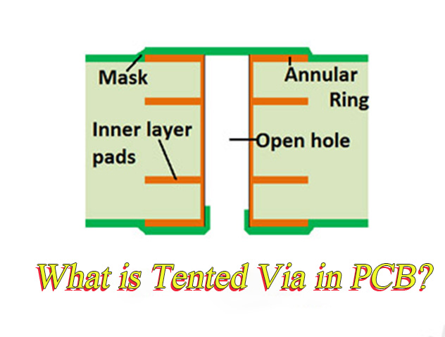
What is Tented Via in PCB?
A tented via is a copper-plated hole fully covered by solder mask. The mask forms a thin “film” over the opening, preventing direct exposure during SMT processing. The via is still electrically functional, but its hole is closed on at least one side by solder mask.
There are three typical variations:
- Fully tented vias – solder mask covers both sides.
- Partially tented vias – solder mask covers one side.
- Tented + filled vias – not fully plugged, but mask covers the top after partial filler.
Because the solder mask closes the hole, the via is protected from unintended solder flow, debris, oxidation, and moisture. This makes the design cleaner and more consistent. Even more, tenting brings visual benefits for silkscreen and component placement, especially when space is tight.
What Are Advantages and Disadvantages of PCB Via Tenting?
- Improved cleanliness: Tented vias block solder from wicking into holes during reflow. This prevents weak joints or missing solder volume on pads nearby.
- Lower risk of bridging: Small vias very close to pads no longer “steal” solder during reflow, which improves yield.
- Smoother assembly: A fully tented surface offers a more even solder mask topography, ideal for high-density layouts.
- Enhanced durability: Mask-covered vias resist oxidation and environmental moisture better than exposed copper.
- Better silkscreen printing: Mask-covered holes allow labels, indicators, or polarity marks to be printed nearby without artwork breaks.
Why Use Tented Vias?
- Prevent solder wicking: Tiny vias near pads can siphon solder away during reflow. Tenting stops that.
- Improve reliability: A covered via has fewer chances of oxidation or contamination.
- Reduce shorts: Vias between dense components often need coverage to prevent unexpected bridging.
- Support miniaturization: Modern PCBs pack many vias under BGAs, modules, and connectors. Tenting keeps these areas stable and clean.
- Enhance solder mask performance: A smoother surface improves automated assembly and reduces defects.
When to Use PCB Via Tenting in PCB Layout?
- Vias are placed close to SMT pads: This stops solder loss and protects pad stability.
- Under a BGA or LGA: Small vias often hide beneath packages to save space. Tenting avoids unintended wicking during reflow.
- The circuit uses fine-pitch components: Dense circuits benefit from a clean, mask-covered surface.
- Via-in-pad is not required: If you do not need filled and plated vias, tenting provides a cost-friendly alternative.
- The PCB requires better environmental protection: Outdoor devices, sensors, or medical equipment benefit from enclosed vias.
- Silkscreen location is limited: Covering vias smooths the area and allows printing over the region.
Tenting Vias vs Plugged Vias: How to Choose?
| Criteria | Tented Vias | Plugged Vias |
| Protection level | Good for general applications | Excellent sealing and higher reliability |
| Solder wicking control | Very effective | Completely eliminated |
| Thermal performance | Standard | Better for high-power or thermal vias |
| Surface smoothness | Smooth, acceptable for most designs | Very smooth; ideal under BGA pads |
| Cost | Low | Higher (due to filler material and extra steps) |
| Recommended via size | 0.2–0.5 mm | 0.1–0.3 mm common |
| Ideal application scenarios | Consumer electronics, IoT devices, general SMT | High-density BGAs, HDI, thermal paths, advanced RF |
| Manufacturing complexity | Low | Medium to high |
| Mask reliability | Depends on registration | Very stable after plugging |
| Best choice when | You need low-cost protection and stable SMT | You need high reliability or via-in-pad |
What Are Design Rules for PCB Via Tenting?
Below Are 12 PCB Via Tenting Design Rules for Your Reference:
1. Solder Mask Expansion: 0 to −2 mil (−0.05 mm)
- The solder mask opening should match the copper pad (0 mil expansion) or shrink slightly (negative expansion). Negative values (−1 to −2 mil) enhance coverage and reduce pinholes, especially for vias <0.35 mm.
2. Recommended Via Hole Diameter
- Optimal finished hole size: 0.2–0.4 mm (preferred: 0.25–0.35 mm) with annular ring 0.1–0.15 mm. Smaller vias tent more easily as mask spans less unsupported area.
3. Avoid Tenting Vias >0.5 mm
- Large vias (>0.5 mm) risk mask cracking or air bubbles. For larger holes, use plugging/filling.
4. Solder Mask Thickness: 15–35 μm
- Standard: 15–25 μm. Critical layers/high-density zones use 25–35 μm for enhanced sealing. Thicker masks require precise curing to prevent lifting.
5. Use LPI Solder Mask
- LPI (Liquid Photoimageable) offers superior adhesion, resolution, and strength vs. dry-film. Ideal for micro-contour tenting.
6. Maintain Clean Spacing Around Vias
- Avoid routing <4 mil from vias. Mask-to-copper clearance ≥3–4 mil prevents fracturing/uneven coverage.
7. Account for Mask Registration Tolerance
- Fabrication shifts (±3 mil) require comfortable spacing to avoid unintended copper exposure.
8. Avoid Tenting Test-Point Vias
- Vias for ICT/testing must remain open. Tented vias cannot ensure reliable probe contact.
9. Add Clear Fab Notes: Specify in drawings
- “Tented vias on both sides” or “Negative mask expansion for vias <0.35 mm” to avoid misinterpretation.
10. Avoid Tenting Vias on Large Copper Planes
- Thermal reliefs prevent uneven curing/voids due to copper heat absorption differences.
11. Control Via-Pad Spacing
- For SMT pads near vias: Pad-to-via spacing >4–6 mil with defined mask fillet prevents solder bridging.
12. Verify via CAM Review
- Pre-production CAM checks confirm correct mask expansion, via size norms, alignment tolerance, and no exposed copper, reducing re-spins and ensuring stable yield.

How to Make Vias Tented?
Below Are Steps to PCB Vias Tented Production Process:
1. Gerber File Output and Verification
- Solder Mask Gerber: When generating Top/Bottom Solder Mask layer Gerber files, confirm no “Thermal Pad” design on via pads to ensure continuous solder mask coverage over via openings.
- Design Rule Verification: Use CAM350 or GC-PowerView tools to perform DRC checks, validating parameters like solder mask-to-copper spacing (≥0.1mm) and solder mask bridge width (≥0.1mm).
- Optical Point Handling: Adjust solder mask opening size for vias near test points or optical alignment marks to ensure automated equipment recognition.
2. Production Preparation: Material and Process Selection
- Solder Mask Material: Use liquid photoimageable solder mask (LPI) with thickness 0.8-1.2mil for coverage and solder resistance. For high-reliability applications (e.g., automotive), UV-curable solder mask may be selected.
- Pre-treatment Process: Conduct micro-etching, acid cleaning, or other pre-treatments to enhance solder mask adhesion. Ensure via surfaces are clean, free of oxide or contaminants.
- Stencil Design: For screen printing, customize stencils to fully cover via areas; for inkjet printing, adjust ink drop spacing and layer height.
3. Solder Mask Application and Curing
- Solder Mask Coating: Apply solder mask uniformly via screen printing, inkjet, or photosensitive coating. Ensure complete ink filling in via areas without bubbles or pinholes.
- Exposure and Development: Use UV exposure machine for pattern exposure, then remove unexposed solder mask with alkaline developer to retain covered vias.
- Curing Treatment: Perform thermal curing (e.g., 150℃×60min) or UV curing in high-temperature ovens to achieve solder mask hardness ≥3H and thermal shock resistance per IPC-SM-840.
4. Quality Control and Inspection
- AOI Inspection: Use automated optical inspection (AOI) to scan solder mask for defects (e.g., exposed copper, thin ink, broken bridges) with accuracy ±0.05mm.
- Cross-section Analysis: Perform metallographic cross-sectioning on critical vias to verify solder mask thickness, coverage integrity, and adhesion strength (e.g., pull test ≥1.5kgf).
- Electrical Testing: Conduct flying probe or ICT testing to confirm no shorts/opens post-tenting, with insulation resistance ≥100MΩ (500V DC).
5. Special Scenario Handling
- High-Density Designs: For microvias (<0.2mm), recommend resin plugging + tenting when using “Via-in-Pad” to avoid solder mask collapse.
- Thermal Management: For vias under high-power devices, evaluate thermal needs—use HASL pads if heat dissipation is required, otherwise maintain tenting.
- Traceability: Batch PCBs must include solder mask lot numbers, curing parameters, and inspection records per ISO 13485/IATF 16949 requirements.
How Much Does PCB Via Tenting Cost?
The cost of PCB via tenting depends on board size, count of vias, solder mask type, and manufacturing class. Fortunately, tenting adds very little cost because it is part of the standard mask process.
| Project Type | Additional Cost for Via Tenting |
| Prototype / small batch | $0 – $15 per order |
| Mid-volume production | $10 – $40 per batch |
| High-volume mass production | $0 – $0.002 per via |
FAQs of PCB Via Tenting
Q1. Should I tent all vias on my board?
A1: Not always. It depends on the purpose of each via. Small vias near pads benefit from tenting, while test-point vias or thermal vias should stay open or be plugged. We help analyze your layout to determine where tenting adds value.
Q2. Is it safe to tent vias under a BGA?
A2: Yes. This is a very common practice when via-in-pad is not needed. Tenting prevents solder from draining into small holes. We ensure the via size and mask alignment support reliable sealing.
Q3. Will solder mask always fully cover small vias?
A3: Most of the time, yes. Vias between 0.2–0.35 mm tent very well. Larger vias may not close completely. We advise optimal via sizes to ensure stable production.
Q4: Do tented vias affect signal integrity?
A4: Only minimally. The thin mask has negligible impact on impedance. If your board needs strict RF performance, we simulate trace and via behavior during stack-up review.
Q5: Is tenting enough for HDI boards?
A5: For many HDI designs, tenting is sufficient. If you have dense BGA packages or need heat dissipation, plugged or plated-over vias may be better. We offer both options and help compare costs and performance.