

How to design a 20 layers HDI PCB? This guide covers stack-up, design, manufacturing, and why our 19+ years of expertise make us your ideal partner.
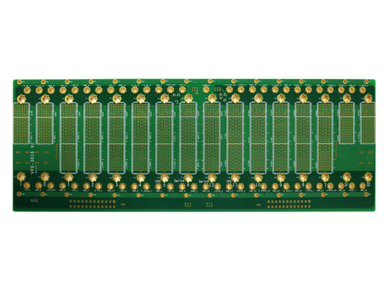
What Is A 20 Layers HDI PCB?
A 20 layers HDI PCB (High-Density Interconnect Printed Circuit Board) is a 20-layer PCB that utilizes microvia technology to achieve high-density wiring. Its features include smaller line widths/spacings (typically ≤75μm), buried and blind via structures, high integration density, and low signal loss. Compared to traditional multilayer PCBs, 20 layers HDI PCB offer superior electrical performance, space utilization, and reliability, and are widely used in high-end fields such as 5G communication, medical equipment, aerospace, and consumer electronics.

20 Layers HDI PCB Stackup
| Layer Range | Material Type | Copper Thickness | Thickness | Function |
| 1-2 | FR4 | 35μm | 200μm | High-speed signal & power delivery |
| 3-4 | PP | None (Insulating Layer) | 100μm | Layer insulation & bonding |
| 5-6 | High-Frequency Low-Loss Substrate | 35μm | 200μm | RF/high-speed traces with low loss |
| 7-8 | PP | None | 100μm | Secondary insulation & microvia support |
| 9-10 | FR4 | 35μm | 200μm | EMC optimization & noise reduction |
| 11-16 | Thin FR4 | 18μm | 150μm | HDI microvias (≤100μm holes, ≤8:1 ratio) |
| 17-18 | PP | None | 80μm | Sub-stack to core bonding |
| 19-20 | FR4 | 35μm | 200μm | Impedance-controlled signal output |
20-Layers HDI PCB Design Technical Parameter
| Parameter | Typical Value/Range |
| Number of Layers | 20 |
| Board Thickness | 1.6mm – 3.0mm (Common: 2.0mm) |
| Material | FR-4 High-Tg (Tg ≥ 170°C) or High-Speed Materials (e.g., Rogers) |
| Copper Weight | Outer: 1oz (35μm), Inner: 0.5oz (17.5μm) |
| Min Trace Width | 0.075mm (3mil) |
| Min Trace Spacing | 0.075mm (3mil) |
| Min Hole Size | Mechanical Drill: 0.2mm, Laser Microvia: 0.1mm (4mil) |
| Via Types | Blind, Buried, Microvias |
| Microvia Size | Diameter: 0.1mm, Depth: ≤0.1mm (per layer) |
| Impedance Control | Single-ended: 50Ω, Differential: 100Ω (±10%) |
| Surface Finish | ENIG, HASL-LF, or OSP |
| Min Pad Size | 0.25mm (Microvia Pad) |
| Lamination Sequence | e.g., 2+N+2 (2 buildup + N core + 2 buildup) |
| Dielectric Constant (Dk) | FR-4: ~4.2, High-Speed: 3.0-3.5 |
| Tg Value | ≥170°C (High-reliability designs) |
| Min Annular Ring | 0.05mm (Microvia) |
| Copper Roughness | ≤1.5μm RMS (Optimized for SI) |
How to Design A 20 Layers HDI PCB?
A detailed design guide 20 layers HDI PCB board:
1. Stack-up Structure Planning
- Layer Allocation Principle: Adopt an alternating “signal layer + plane layer” structure. Recommend 10-12 signal layers + 8-10 plane layers (power/ground). Example: Top signal layer, GND layer, signal layer, VCC layer, signal layer, GND layer… Bottom signal layer.
- Symmetry Design: Ensure mirror symmetry of layers (e.g., layer 3 matches layer N-2) to prevent board warpage. Layer stack thickness must align with copper thickness (e.g., 50-100μm dielectric thickness for 18μm copper).
- Material Selection: Use low-loss substrates (e.g., Panasonic M6/M7) for high-frequency applications; standard FR-4 suffices for general cases. Inner layers should use low dielectric constant (Dk) materials to minimize signal delay.
2. Microvia and Buried Via Technology
- Via Type Selection: Prioritize laser-drilled blind/buried vias (diameter ≤100μm) to reduce through-hole ratios. Example: 1st-order HDI uses 1+N+1 structure (top blind via → inner layer); 2nd-order HDI uses 2+N+2 structure (top blind via → inner buried via → bottom).
- Via Dimensions: Minimum via size must match manufacturing capabilities (typically ≥75μm), with spacing ≥100μm. Blind vias should be staggered to avoid stress concentration.
- Plating Process: Use electroless copper + electroplating to achieve >80% via fill ratio, preventing voids that compromise reliability.
3. Signal Integrity
- Impedance Control: All signal layers require strict impedance design (single-ended 50Ω±10%, differential 100Ω±10%). Calculate trace width/spacing using tools like Polar SI9000, accounting for substrate Dk and copper roughness.
- Crosstalk Mitigation: Sensitive signals (e.g., high-speed differential pairs) follow the 3W rule (trace spacing ≥3x trace width). Add ground shielding traces if necessary. Differential pairs must match lengths (error ≤5mil); inner-layer pairs prefer stripline structures.
- Return Path Planning: Ensure high-speed signals have continuous reference planes (ground or power) beneath them, avoiding plane splits. Critical signals (e.g., clocks) should route in inner layers to reduce radiation.
4. Power Integrity
- Power Plane Partitioning: Segment power planes by module (e.g., CPU core voltage, I/O voltage) to prevent plane fragmentation. Use anti-pads to control copper-to-via clearance (typically ≥20mil).
- Decoupling Capacitor Placement: Position high-frequency decoupling caps (0.1μF) near chip power pins; place bulk caps (≥10μF) at power entry points. Route caps with minimal loop area using the “closest principle.”
- Power Plane Thickness: Recommend ≥2oz (70μm) copper for power layers to lower impedance; widen copper traces or use copper bars for high-current paths.
5. Thermal Management
- Heat Dissipation Design: Add thermal vias (via farms) beneath high-power devices (e.g., BGA packages) to form heat channels. Use inner thermal layers and high-thermal-conductivity substrates (e.g., TGF).
- Thermal Via Arrays: Densely arrange thermal vias (spacing ≤1mm) in heat-source areas. Fill vias with thermal paste or copper paste to enhance heat transfer.
- Temperature Monitoring: Reserve thermistor pads in critical zones; design considering airflow paths to prevent heat buildup.
6. Manufacturing Constraints and DFM Validation
- Trace/Space Dimensions: Minimum trace width/spacing ≥3mil (matching manufacturing capabilities). Use negative-tone processes in dense areas to reduce etching defects.
- Soldermask and Marking: Soldermask openings must exceed pads by 10μm to avoid bridging; ensure clear silkscreen markings without covering test points.
- DFM Checks: Use tools like Allegro or Altium for DRC/DFM validation, focusing on: minimum via size/spacing, impedance matching, copper connectivity, and thermal via placement.
7. Testing and Debugging
- Test Point Design: Reserve test points (spacing ≥100mil) for critical signal pins using test fixtures or flying probes.
- Simulation Validation: Perform SI/PI simulations (e.g., HyperLynx, ADS) to identify reflections, crosstalk, or ground bounce early.
- Prototype Verification: After fabricating engineering samples, conduct electrical tests, thermal imaging, and mechanical tests (e.g., thermal shock, vibration) to validate design compliance.
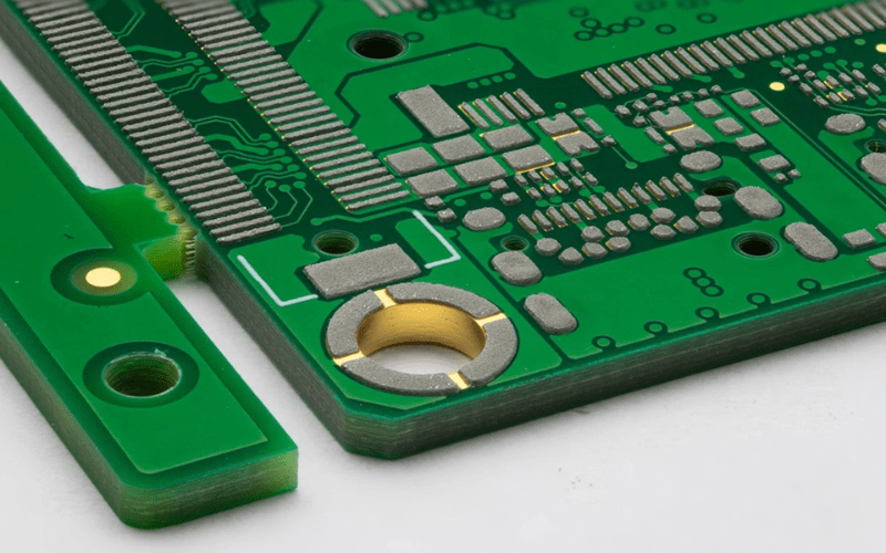
How to Make A 20 Layers HDI PCB?
20-Layer HDI PCB Production Process:
1. Design File Verification and Optimization
- Receive Gerber files, drilling data, and stack-up diagrams. Use EDA tools (e.g., Altium, Cadence) for DRC checks to ensure trace width/spacing, via dimensions, and other parameters meet manufacturing capabilities.
- Optimize layout and routing to minimize crosstalk. Plan blind/buried via positions and interlayer connection schemes to align with HDI process requirements (e.g., 1+N+1 or 2+N+2 structures).
2. Substrate Preparation and Pretreatment
- Select low-loss high-speed materials (e.g., Panasonic M6/M7) or standard FR-4 substrates. Cut inner-layer cores (Copper Clad Laminate, CCL) to 0.1–0.3mm thickness per stack-up design.
- Perform black oxide or brown oxide treatment on cores to enhance interlayer adhesion. Prepare outer-layer copper foils (e.g., 18μm or 35μm thickness) with surface cleanliness meeting IPC-A-600 standards.
3. Inner Layer Image Transfer and Etching
- Apply dry film photoresist to inner-layer cores. Transfer design patterns via exposure and development to create etch-resistant masks.
- Etch unprotected copper using acidic solutions (e.g., CuCl₂) to form inner-layer circuits. Remove photoresist (stripping) and conduct AOI inspection to verify no open/short defects.
4. Lamination and Blind/Buried Via Creation
- Stack inner-layer cores, prepregs, and copper foils in sequence. Use vacuum presses for high-temperature/pressure lamination to form multilayer substrates.
- Drill through-holes (diameter ≥0.2mm) mechanically. Create blind (diameter ≤0.1mm) and buried vias via laser drilling (CO₂/UV lasers) with positional accuracy ≤±0.05mm.
5. Via Metallization and Plating
- Perform chemical copper deposition (PTH) on drilled substrates to form conductive via walls. Electroplate copper to design thickness (≥20μm) ensuring >80% fill ratio.
- Use pulse plating or via-filling techniques to minimize voids. Post-plating treatments include degreasing and micro-etching to remove surface contaminants.
6. Outer Layer Image Transfer and Etching
- Repeat inner-layer processes: apply dry film, expose, develop, and etch outer-layer copper foils using alkaline solutions (e.g., NH₃·H₂O) to form outer circuits.
- Strip photoresist and conduct secondary AOI inspection to confirm outer-layer trace accuracy.
7. Soldermask and Surface Finish
- Apply liquid photosensitive soldermask ink. Expose and develop to create protective patterns (20–30μm thickness). Soldermask openings should exceed pad dimensions by 10–15μm.
- Apply surface finishes (e.g., ENIG, OSP, immersion gold) per requirements. Immersion gold thickness should be 0.05–0.2μm for reliable soldering.
8. Profiling and Electrical Testing
- Shape PCBs using CNC routing or laser cutting to meet contour specifications. Edges must be smooth and burr-free per IPC-6012.
- Conduct flying probe or fixture testing to verify electrical performance (e.g., opens, shorts, impedance). Perform AOI and X-ray inspections to check via fill and layer alignment.
9. Final Inspection and Packaging
- Perform visual checks, dimensional measurements, and performance sampling to confirm no delamination, voids, or pad lifting. Compliance with IPC-A-600 and customer-specific criteria is required.
- Package using moisture-barrier bags (e.g., vacuum packaging with desiccants). Label with product model, batch, and manufacturing date. Include documentation (e.g., COC, test reports) per customer requirements.
Why Choose EBest Circuit (Best Technology) for 20 Layers HDI PCB Manufacturer?
Reasons to choose EBest Circuit (Best Technology) for 20 layers HDI PCB manufacturer:
- Cost-Competitive Pricing with 15-20% Savings: Benchmarked against industry averages, our pricing model delivers 15-20% cost savings without compromising quality. For a 20-layer HDI prototype, customers report average savings of 800−1,200 per batch compared to Tier-1 competitors.
- 99.8% Yield Rate: Strict process controls (ISO 9001:2015/ISO 14001 certified) and automated optical inspection (AOI) systems ensure <0.2% defect rate. Our 100% electrical testing protocol eliminates open/short defects, backed by a 2-year warranty for volume orders.
- Impedance Testing with ±5% Accuracy: Every 20-layer HDI board undergoes Time-Domain Reflectometry (TDR) testing with Polar Instruments SI9000. Our impedance control meets IPC-6012 Class 3 standards, with single-ended 50Ω±5% and differential 100Ω±5% tolerance.
- 19-Year Expertise in 20-Layer HDI Manufacturing: With 19 years of specialized HDI experience, we’ve delivered over 120,000 20-layer boards for 800+ global clients. Case studies show 30% shorter design cycles and 40% higher first-pass success rates for complex HDI projects.
- Free DFM Analysis Saving 30% Design Time: Complimentary Design-for-Manufacturing checks using Siemens Xpedition identify 50+ potential issues (e.g., via spacing, trace width). Clients report 30% reduction in design iterations and 50% faster time-to-market.
- 72-Hour Rapid Prototyping with 99.2% On-Time Delivery: Our accelerated workflow delivers 20-layer HDI prototypes in 72 hours – 40% faster than industry norms. With a 98% on-time delivery rate, engineers receive samples for testing 3 days after final Gerber approval.
- Advanced Material Portfolio with Low-Loss Substrates: Offering Panasonic M6/M7, ITEQ IT-180A, and Rogers RO4350B materials, our boards achieve <0.002 Df loss tangents for 5G/mmWave applications. Material-specific stack-up optimization reduces signal loss by 35% at 28GHz.
- Thermal Management Solutions with 20% Cooling Efficiency: Embedded thermal vias and copper-invar-copper (CIC) cores reduce junction temperatures by 20°C. Our via-farm designs achieve >150W/m² thermal conductivity, validated through ANSYS thermal simulation reports.
Our Impedance Check Process for 20 Layers HDI PCB
1. Pre-Test Parameter Calibration: Use Polar Instruments SI9000 and TDR systems to calibrate test fixtures with ±1% accuracy, ensuring all impedance targets meet IPC-6012 Class 3 standards. This step guarantees measurement consistency across all 20 layers.
2. Automated Coupon Extraction: Implement laser-guided systems to precisely extract 100μm-wide test coupons from each layer, minimizing human error and ensuring representative sampling of signal/power planes.
3. Multi-Frequency TDR Scanning: Conduct Time-Domain Reflectometry at 1GHz, 3GHz, and 5GHz frequencies using Keysight DCA-Z systems. This multi-frequency approach detects impedance variations across the entire bandwidth, crucial for high-speed digital designs.
4. Real-Time Data Analysis: Integrate test results with Siemens EDA tools to generate 3D impedance plots and statistical process control (SPC) charts. Engineers receive immediate pass/fail notifications with ±3% tolerance windows.
5. Layer-Specific Validation: Perform differential pair testing with 100Ω±3% tolerance on all 20 layers, using microsection analysis to verify copper plating thickness and dielectric spacing. This ensures 100% compliance with HDI signal integrity requirements.
6. Automated Report Generation: Generate ISO 17025-certified test reports with traceable data logs, including raw TDR waveforms and statistical process control metrics. Clients receive these reports within 2 hours post-testing via secure cloud portal.
7. Continuous Process Optimization: Leverage machine learning algorithms to analyze historical test data, reducing impedance variation by 40% through adaptive laser drilling and plating parameter adjustments.
Our HDI PCB Production Capability
| Parameter | Production Capability |
| Copper Thickness | Outer Layer:1oz~30oz, Inner Layer:0.5oz~30oz |
| Min Line Width/Line Space | 3/3mil |
| Min Hole Diameter | 4mil |
| PTH/NPTH Dia Tolerance | PTH: ± 3mil; NPTH: ±2 mil |
| Surface Treatment | ENIG(Au 4u’’),ENEPIG (Au 5u’’) Gold finger/Hard Gold Plating(Au 50u’’), HASL /LF HASL, OSP, Immersion Tin, Immersion Silver |
How to Get A Quote for Your HDI PCB Project?
Here are steps to get a quote for HDI PCB project:
1. Define Technical Specifications: layer count, copper thickness (outer/inner layers), min line width/space (e.g., 3/3mil), min hole diameter (e.g., 4mil), PTH/NPTH tolerances, surface finishes (ENIG, ENEPIG, etc.), and material type.
2. Identify HDI-Capable Manufacturers: Research suppliers with proven HDI expertise. Check their production capabilities (e.g., 3/3mil line/space, 4mil microvias) and quality certifications (ISO, IPC).
3. Prepare Documentation: Provide Gerber files, BOM (Bill of Materials), and detailed drawings. Include stack-up information, impedance requirements, and testing specifications (e.g., electrical tests, X-ray inspection).
4. Request a Quote (RFQ): Contact manufacturers via email/online portal. Share your specifications and ask for a formal quote. Include quantity, desired lead time, and any special requirements (e.g., RoHS compliance).
5. Evaluate Quotes: Compare pricing, lead times, and terms. Assess technical capabilities (e.g., can they handle 4mil holes?) and quality control processes. Request samples or case studies if needed.
6. Negotiate and Confirm: Discuss pricing, payment terms, and delivery schedules. Clarify warranty, after-sales support, and revision policies. Sign a contract once all details are finalized.
7. Provide Feedback for Optimization: Share post-quote feedback with the manufacturer to refine designs or reduce costs (e.g., adjusting layer count or surface finish).
Welcome to contact us if you have any request for HDI PCB board: sales@bestpcbs.com.
Tags: 20 Layers HDI PCB, 20 Layers HDI PCB Design, 20 Layers HDI PCB Design Guide, 20 Layers HDI PCB Manufacturer, 20 Layers HDI PCB Stackup