

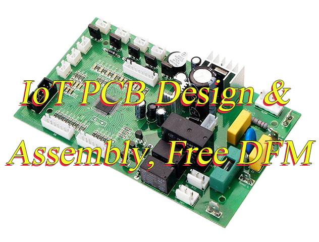
How to design an IoT PCB? Let’s discover benefits, applications, design guide and optimization strategies, assembly process for IoT circuit board.
Are you troubled with these problems?
- Does data transmission in IoT devices become unstable and frequently disconnect due to PCB signal interference?
- Can PCB design achieve miniaturization while integrating complex IoT sensors, avoiding a sharp drop in yield during mass production?
- Does the supply chain response speed for multiple batches of small orders slow down product iteration cycles?
As an IoT PCB Manufacturer, EBest Circuit (Best Technology) can provide you service and solutions:
- High-Frequency Micro-Amplitude Circuit Optimization: Ensuring Wi-Fi/Bluetooth module signal integrity and reducing bit error rate through precise impedance control processes.
- HDI Rapid Prototyping: Achieving extreme compression of sensor modules using blind and buried vias and microvia stack-up technology, accelerating prototype verification.
- Flexible Production System: A dynamic material early warning mechanism supports 48-hour turnaround for urgent orders, adapting to the agile development needs of smart home and wearable devices.
Welcome to contact us if you have any inquiry for IoT PCB design, prototyping, assembly: sales@bestpcbs.com.
What Is a PCB in IoT?
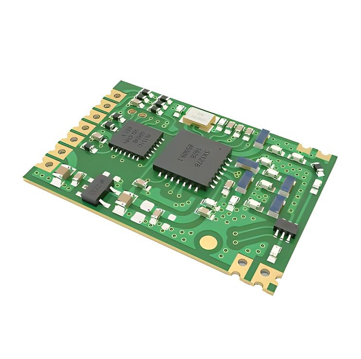
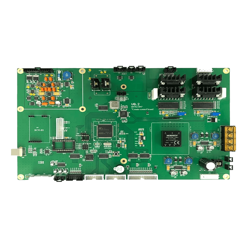
IoT PCB is the core carrier connecting electronic components. It integrates components such as sensors, microcontrollers, and communication modules into a compact space through precise wiring, realizing data acquisition, processing, and transmission functions. At the same time, it must meet the characteristics of low power consumption, high reliability, and miniaturization, and is the key hardware foundation for IoT devices to achieve intelligent interconnection.
What Are Advantages of IoT PCB?
Benefits of IoT PCB board:
- Miniaturization Support: Utilizing High-Density Interconnect (HDI) technology, microvia design, and fine linewidth/spacing processes, combined with ultra-small packaged components such as 0201/01005-level resistors and capacitors, and CSP/WLP, complex functions are implemented in a very small space, adapting to the size requirements of wearable devices and micro-sensors.
- Ultra-Low Power Operation: Integrating a low quiescent current PMIC (Power Management Chip), an ultra-low power MCU (Microcontroller), and a high-efficiency DC-DC converter, with a finely designed power domain management and deep sleep wake-up mechanism, reducing overall power consumption and extending battery or energy harvesting system lifespan.
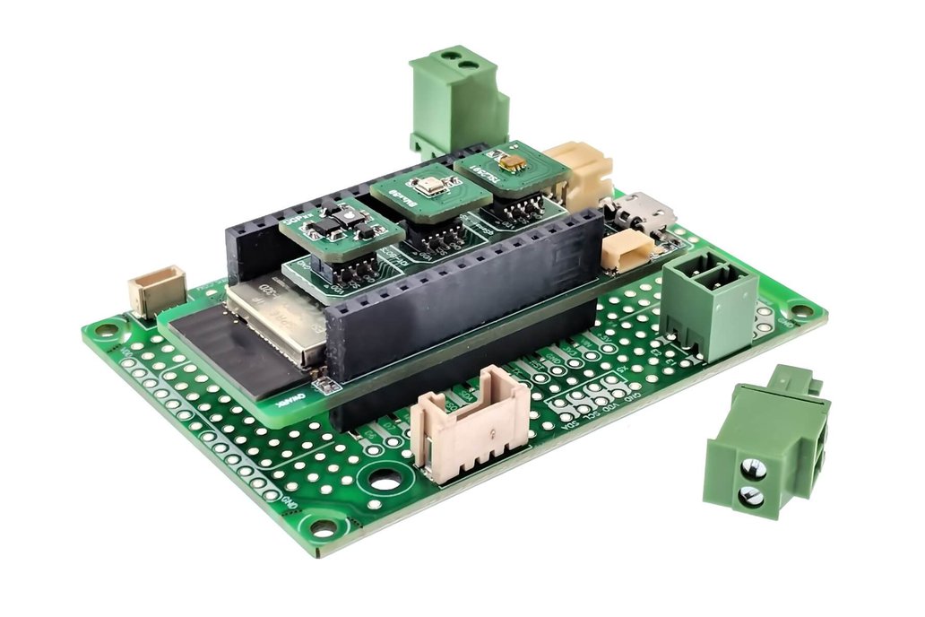
- Multi-Mode Wireless Connectivity: Natively integrating and optimizing RF circuitry for wireless protocols such as Wi-Fi, Bluetooth LE, LoRa, NB-IoT, and Zigbee, ensuring 50-ohm impedance control of the antenna interface and signal integrity, enabling flexible device access to various networks.
- Diverse Sensor Interfaces: Providing analog/digital sensor interface circuitry, supporting direct connection and signal conditioning (through integrated AFE analog front-end) for various physical quantity sensors such as temperature, humidity, light, motion, and environment, simplifying the sensing layer design.
- Environmental Adaptability and Reliability: Utilizing industrial-grade/wide-temperature-range components and high-Tg board materials, combined with conformal coating for moisture and dust protection and vibration/shock resistance, ensures long-term stable operation in harsh or unattended environments.
- Hardware-Level Security Mechanisms: Integrating a hardware security element (SE), circuit design supporting secure boot and secure OTA firmware updates, and employing physical anti-tamper detection and shielding measures, providing a physical foundation for device authentication, data encryption, and tamper prevention.
- Manufacturing Cost and Efficiency Optimization: Adhering to DFM (Design for Manufacturability) principles, prioritizing cost-effective standard components and mature processes (such as primarily 4-layer boards), and adopting a modular (core board + baseboard) design improves production yield and reduces material and manufacturing costs for large-scale deployment.
- Enhanced Functional Integration: Efficiently integrating high-speed digital, analog, RF, and power mixed-signal circuits within a limited space, reducing the number of external components and system complexity through precise layer stack-up planning and routing strategies (such as blind and buried via technology).
What Are Applications of IoT PCB?
Applications of IoT PCB board:
- Smart wearable devices – smartwatches and health monitoring bracelets
- Environmental monitoring sensor networks – smart agriculture soil/weather stations and building air quality monitoring points
- Industrial equipment predictive maintenance systems – motor vibration monitoring sensors and production line status monitoring nodes
- Smart home terminals – networked thermostats, smart door locks, and security sensors
- Logistics asset tracking tags – cargo tracking devices and container status monitoring terminals
- Portable medical monitoring devices – remote ECG monitors and blood glucose data acquisition terminals
- Smart utility meters –remotely read water meters, electricity meters, and gas meters
- Vehicle-to-everything (V2X) terminals –vehicle telematics units (T-Boxes) and tire pressure monitoring modules
- Smart city infrastructure – smart street light controllers and parking space detection sensors
- Industrial IoT gateways – edge computing nodes connecting field devices to cloud platforms
How to Design an IoT PCB?
Below is a detailed design guide for IoT PCB board for your reference:
1. Hardware Selection and Modular Design
Core Component Selection
- Microcontroller (MCU): Prioritize low-power, high-integration ARM Cortex-M series (e.g., STM32L4/STM32U5) or RISC-V architecture chips supporting Bluetooth/Wi-Fi/NB-IoT protocols. Verify long-term supply guarantees (LTS) and ecosystem support (e.g., SDK, development tools).
- Sensor Modules: Select digital/analog sensors (e.g., temperature, acceleration, gas sensors) based on application scenarios, ensuring interface compatibility (I²C/SPI/UART) and calibration accuracy requirements.
- Wireless Modules: Evaluate RF performance (TX power, receive sensitivity), power modes, and certification standards (FCC/CE/IC). Prefer multi-band, low-power modules (e.g., Semtech LoRa SX1276).
Modular Design Principles
- Implement standard interfaces (e.g., MIPI, USB Type-C) for plug-and-play functionality of modules (power, communication, sensors), enhancing maintainability and scalability.
- Reserve test points (TP) and debug interfaces (e.g., JTAG/SWD) for post-debugging and firmware updates.
2. Circuit Design and Low-Power Optimization
Low-Power Architecture Design
- Implement multi-level power management strategies: dynamic voltage frequency scaling (DVFS), sleep/deep sleep mode switching, and RTC timer wake-up mechanisms.
- Use low-power components (e.g., ultra-low leakage MOSFETs, low-power op-amps) and avoid leakage current paths.
Anti-Interference and Signal Integrity
- EMC Design: Comply with CISPR 22/EN 55022 standards. Suppress high-frequency noise via filter capacitors, ferrite beads, and common-mode chokes. Key signal lines (e.g., clocks, RF) use differential routing with controlled impedance (50Ω/100Ω).
- Power Integrity: Utilize multi-stage filtering (π-type networks), power plane partitioning (digital/analog zones), and avoid ground bounce and power noise.
3. Layout and Routing Strategies
Layer Planning and Thermal Management
- Adopt 4-layer or higher PCB structures: top/bottom layers for signal routing, inner layers for power/ground planes. Reduce signal crosstalk.
- Place high-power devices (e.g., power amplifiers) with thermal vias or thermal pads, paired with thermal interface materials (e.g., thermal pads) for optimized heat conduction.
Routing Rules
- High-speed signal lines (e.g., SPI, SDIO) use serpentine routing for timing control, avoiding signal reflections. RF lines remain short and straight, distanced from digital lines to minimize coupling.
- Critical trace widths match impedance requirements (e.g., 50Ω microstrip) and are validated via TDR testing.
- Avoid sharp-angle traces to reduce signal radiation and impedance discontinuities.
4. Power System Design
Power Architecture Selection
- Choose linear regulators (LDOs) for low-noise scenarios or switching regulators (DC-DCs) for high-efficiency conversion based on application needs.
- Battery-powered systems require protection circuits (overcharge/over-discharge/short-circuit) with low-battery detection and sleep mode switching.
Power Path Design
- Implement power path management for automatic switching between battery and external power (e.g., USB), preventing reverse current flow.
- Isolate critical chips with independent power domains using inductors/capacitors to reduce noise coupling.
5. Signal Integrity and EMC Design
High-Speed Signal Processing
- Match impedance (source/terminal) for high-frequency signals (e.g., RF, high-speed digital) to minimize reflections and ringing.
- Shield sensitive circuits with enclosures or metal casings to reduce external interference.
EMC/EMI Compliance Design
- Conduct EMC pre-compliance analysis via simulation tools (e.g., Ansys HFSS, Altium Designer) to optimize layout and shielding.
- Add common-mode chokes and TVS diodes to critical interfaces (e.g., USB, Ethernet) for ESD and surge protection.
6. Testing and Verification Process
Functional Testing
- Perform unit, integration, and system-level testing to validate hardware functionality, communication protocols, and power performance.
- Analyze signal integrity using logic analyzers, oscilloscopes, and spectrum analyzers.
Environmental and Reliability Testing
- Follow IEC 60068 standards for environmental testing (temperature, vibration, humidity) to ensure stability across conditions.
- Conduct accelerated life testing (ALT) and thermal cycling to validate solder joint and component reliability.
7. Environmental and Design for Manufacturing (DFM/DFA)
Environmental Standards
- Comply with RoHS, REACH, and other regulations. Use lead-free solder and eco-friendly materials.
- Prioritize recyclable materials and low-toxicity chemicals to minimize environmental impact.
Design for Manufacturing
- Adhere to IPC-2221/IPC-2222 standards to optimize PCB dimensions, pad spacing, and trace widths for improved manufacturing yield.
- Use DFM tools (e.g., Altium Designer DFM, Mentor Graphics) for manufacturability analysis, avoiding design flaws (e.g., acid traps, missing pads).
8. Documentation and Collaboration Tools
Design Documentation Management
- Use version control systems (e.g., Git) to manage schematics, PCB layouts, and BOM files for traceability.
- Generate detailed design documentation (schematics, PCB layouts, test reports) for team collaboration and maintenance.
Collaboration Tools
- Leverage cloud-based platforms (e.g., Eagle Upverter) for real-time collaboration and design reviews.
- Utilize project management tools (e.g.,Trello) to track design progress and issue resolution.
IoT Circuit Board Design Consideration
EMC Optimization Design
- High-frequency signal path control: Use differential pair routing (e.g., LVDS, USB3.0) to reduce crosstalk. Critical traces (e.g., RF modules, clock lines) require length matching (error ≤5%) to avoid antenna effects.
- Filtering and shielding measures: Parallel X/Y capacitors (e.g., 100nF+10μF combination) at power entry points. Sensitive circuits (e.g., ADC sampling) adopt metal shielding cans, with continuous ground planes connected to the main ground via single-point grounding to prevent ground bounce noise.
Low-Power Dynamic Power Management
- Multi-level power domain partitioning: Set independent power domains based on chip power characteristics (e.g., STM32L low-power MCUs). For instance, sensor modules use LDOs (drop ≤200mV), while wireless modules adopt high-efficiency DC-DC converters (efficiency ≥90%).
- Dynamic voltage frequency scaling (DVFS): Adjust core voltage dynamically (e.g., 1.8V→0.9V) in tandem with load changes (sleep/wake modes), paired with GPIO configurations for fast wake-up (≤10μs).
- Battery life optimization: Design CC/CV charging circuits for lithium batteries (e.g., ER14505) to avoid overcharge (≤4.25V) and over-discharge (≥2.5V), extending device endurance (≥5 years in typical scenarios).
Wireless Module Layout and Antenna Design
- Antenna isolation and matching: Keep antenna areas away from metal objects (distance ≥λ/4). Use π-type matching networks (inductor+capacitor) to tune impedance to 50Ω, with S11 ≤-10dB (in-band).
- Multi-protocol coexistence strategy: For 2.4GHz bands (Wi-Fi/BLE/Zigbee), employ TDMA or SAW filters to minimize mutual interference, ensuring RSSI ≥-80dBm.
- Anti-interference design: Set guard bands (width ≥2mm) at PCB edges to prevent high-frequency signals from crossing split ground planes. Critical RF paths use microstrip lines (50Ω±10% impedance).
Design for Manufacturing (DFM) and Test (DFT)
- DFM rule verification: Conduct DRC checks (e.g., line width/spacing ≥6mil via Altium Designer/OrCAD). Copper thickness ≥1oz meets current-carrying needs; pad dimensions align with IPC-7351 standards (e.g., QFN pad spacing error ≤±0.05mm).
- Test point design: Place test probe points (spacing ≥100mil) at critical nodes (power, ground, signal lines) for 100% electrical continuity verification via ICT (e.g., flying probe testing).
- Thermal design validation: Use ANSYS Icepak for thermal simulation of power devices (e.g., MOSFETs), ensuring junction temperature ≤125°C (Ta=85°C environment). Thermal via arrays density ≥50 vias/cm?.
Hardware Security and Anti-Tamper Design
- Data encryption module: Integrate hardware encryption engines (e.g., AES-128/256) with secure memories (e.g., ATECC608) to protect keys (≥256-bit), preventing side-channel attacks (e.g., power analysis).
- Physical anti-tamper measures: Deploy anti-tamper circuits (e.g., capacitive sensors) around critical chips (e.g., MCUs). Trigger data wipe and device lock upon casing breach.
- Supply chain security: Use unique device IDs (UIDs) and digital signatures (e.g., ECDSA) to verify firmware authenticity, blocking malicious code injection.
IoT PCB Assembly Process
Below is a detailed guide for IoT PCB assembly process:
1. Material Preparation and Verification
- Incoming Quality Control (IQC): Strictly inspect PCB substrate impedance (verified by TDR for ±5% accuracy) and warpage (meeting IPC-6012 standard ≤0.75%); validate 01005/0201 component package dimensions and RF module S-parameters (e.g., S11/S21 initial performance).
- Moisture Sensitive Devices (MSD) Control: Bake moisture-sensitive components like BGA and CSP according to MSL levels (e.g., 125°C/24h for BGA), with smart storage systems monitoring exposure time.
2. Solder Paste Printing
- Stencil Process: Laser-cut ultra-thin stencil (0.1-0.13mm) with micro-apertures matching 01005 components (trapezoidal aperture design, 1:1.2 opening ratio), electropolished for Ra≤0.5μm wall smoothness.
- Vision Alignment System: High-precision dual-camera Mark point positioning (±10μm accuracy), dynamic compensation for PCB warpage; 3D SPI monitors solder paste thickness (target 4-6μm) and provides feedback on squeegee pressure curves.
3. Surface Mount Technology (SMT)
- High-Speed Mounting Strategy: Micro-components (e.g., 01005/0201) follow a “small-first, large-second” sequence with ±15μm placement head accuracy; RF components (inductors/capacitors) are prioritized to minimize thermal impact.
- High-Precision Placement Technology: BGA/LGA components utilize 3D laser calibration systems for real-time X/Y/Z axis offset compensation; QFN component bottom pads are verified for coplanarity via infrared thermal imaging.
4. Reflow Soldering
- Temperature Profile Control: Customized profiles based on solder paste specifications and component temperature tolerance, with peak temperatures of 235-245°C and liquidus times of 30-45s; nitrogen atmosphere reduces oxidation (oxygen content ≤50ppm).
- Cooling Zone Slope Management: Cooling rate controlled at -2~-5°C/s to prevent thermal stress damage; furnace temperature testers validate actual profiles against set parameters.
5. Automated Optical Inspection (AOI)
- Post-Solder Defect Detection: X-ray and AI for BGA solder joint inspection; 3D solder paste inspection predicts bridging/solder ball defects, with big data analyzing correlations between printing parameters and defects.
6. Through-Hole and Selective Soldering
- Wave Soldering Process: Dual-wave soldering (preheat/main wave) with nitrogen protection minimizes through-hole component solder voids; selective soldering fixtures consider thermal capacity matching to avoid SMD component overheating.
- Hand Soldering Rework: Low-residue solder wire (e.g., RMA type) and micro-manipulation stations for micro-component rework, with temperatures ≤350°C to prevent substrate damage.
7. Cleaning and Decontamination
- Precision Cleaning Process: Medical-grade IoT boards use water-based cleaners (e.g., Tergo series) with 40kHz ultrasonic oscillation, validated by SIR testing (surface insulation resistance ≥10⁹Ω).
8. Coating and Protection
- Conformal Coating Application: Robotic arms control coating thickness (50-100μm), with UV-curable coatings achieving 30-second curing; silicone coatings offer -60~200°C wide-temperature performance.
- Underfill Process: BGA component underfill via capillary action, with UV/thermal dual-cure adhesives ensuring complete filling; reliability verified by accelerated aging tests (-40~125°C/1000 thermal cycles).
9. Functional Circuit Test (FCT) and RF Calibration
- Power Management Testing: Dynamic current testers validate μA-level standby current, with power ripple analyzers detecting switching noise; low-power mode switching time ≤1ms.
- RF Performance Verification: VNA tests antenna impedance matching (Smith chart, target VSWR≤1.5); Wi-Fi module transmit power meets FCC/CE standards, with receiver sensitivity better than -90dBm.
- Over-the-Air (OTA) Testing: Chamber environments validate wireless firmware update rates (e.g., BLE 2Mbps mode), with channel simulators testing multipath fading immunity.
10. Final Inspection and Packaging
- Visual Re-inspection Standards: Manual inspection with 10-20X magnifiers checks coating integrity, with label placement error ≤1mm; metallographic microscopes verify solder joint microstructures (e.g., IMC layer thickness).
- Burn-in Testing: High-temperature burn-in (85°C/85% RH for 168 hours) screens for early failures; critical products undergo HAST testing (130°C/85% RH/96h) for accelerated life verification.
Why Choose EBest Circuit (Best Technology) as IoT PCB Assembly Manufacturer?
Reasons why choose us as IoT PCB assembly manufacturer:
- Free DFM (Design for Manufacturing) analysis: Professional front-end design verification to identify process risks early, reduce late-stage design modification costs, and help international engineers optimize design efficiency.
- Rapid lead time guarantee: Leveraging intelligent production line scheduling to achieve 7-10 day fast delivery for conventional IoT PCB assembly, with emergency order response time shortened to 48 hours.
- 99.2% on-time delivery rate: Real-time tracking of production nodes through MES systems, combined with intelligent warehousing and logistics coordination, ensures zero delays for overseas client project schedules.
- Full batch inspection quality commitment: Triple inspection system of AOI + X-ray + flying probe testing achieves 100% full inspection per batch, with defect rate below 50ppm.
- International standard quality control process: Strict adherence to IPC-A-610E Class 2/3 standards, implementing 18 quality gates from IQC to OQC, ensuring compliance with EU RoHS and REACH environmental requirements.
- Transparent cost structure: Detailed quotation and cost analysis reports provided, no hidden fees, supporting price gradient optimization for small-batch prototyping and mass production.
- Professional technical support team: Bilingual engineers available 24/7 for online support, assisting with technical challenges in overseas projects such as RF calibration and fine-pitch soldering.
- Environmentally compliant and sustainable production: Lead-free soldering processes and recyclable packaging, ISO 14001 certified, meeting environmental access thresholds for European and American markets.
- Cost-effective solutions: Process optimization and economies of scale reduce unit costs, offering price competitiveness on par with international manufacturers while ensuring quality, enhancing client product market profitability.
Our PCBA Manufacturing Capabilities
| Item | Capabilities |
| Placer Speed | 13,200,000 chips/day |
| Bare Board Size | 0.2 x 0.2 inches – 20 x 20 inches/ 22*47.5 inches |
| Minimum SMD Component | 01005 |
| Minimum BGA Pitch | 0.25mm |
| Maximum Components | 50*150mm |
| Assembly Type | SMT, THT, Mixed assembly |
| Component Package | Reels, Cut Tape, Tube, Tray, Loose Parts |
| Lead Time | 1 – 5 days |
How to Get A Quote For IoT PCB Board Project?
To obtain a quote for an IoT PCB board project, submit the following essential checklist items:
- Design Files: Provide complete Gerber files, BOM (Bill of Materials) list, coordinate files, and circuit schematics for accurate design interpretation by manufacturers.
- Board Specifications: Specify PCB dimensions (length × width × thickness), number of layers (e.g., 4-layer/6-layer), substrate material type (e.g., FR4, aluminum substrate, high-frequency materials), and surface finish processes (e.g., HASL, ENIG, OSP).
- Process Parameters: Indicate minimum trace width/spacing, minimum hole size (including through-hole/blind via/buried via), impedance control requirements, copper foil thickness, and special process needs (e.g., immersion gold, thick copper plating, back drilling).
- Production Quantity: Clarify order volume (e.g., small-batch prototype, large-scale mass production) and batch delivery requirements, which impact unit costs.
- Delivery Timeline: Specify the required lead time from order placement to delivery (e.g., 7-day rapid board, 15-day standard), noting that urgent orders may incur additional fees.
- Testing Standards: State whether flying probe testing, ICT (In-Circuit Testing), AOI (Automated Optical Inspection), or functional testing is required to ensure product quality compliance.
- Packaging and Logistics: Describe packaging methods (e.g., anti-static bags, vacuum packaging) and transportation modes (air/sea/land freight), with any associated costs confirmed in advance.
Welcome to contact us if you have any request for IoT PCB: sales@bestpcbs.com.
Tags: IoT PCB, IoT PCB Assembly, IoT PCB Design